PCB Return Path and Via Inductance High Speed Rules
This comprehensive guide covers essential PCB Return Path and Via Inductance High Speed Rules for hardware engineers. In modern design, ensuring a continuous PCB return path and minimizing via inductance are critical to achieving pristine signal integrity and passing strict EMI compliance testing.
Understanding the PCB Return Path: Foundation of Signal Integrity
The Principle of Least Inductance
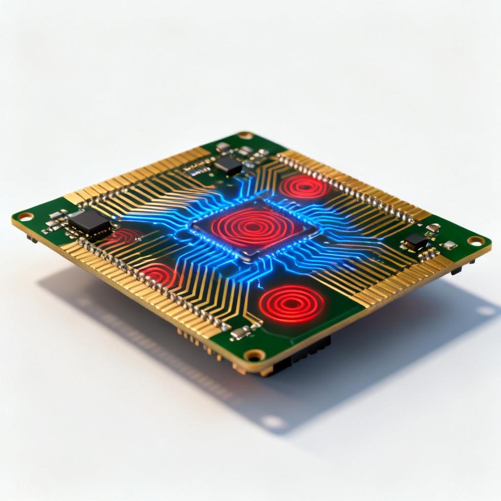
At high frequencies, current follows the path of least inductance. The PCB return path must flow directly under the signal trace on an adjacent reference plane to minimize loop area and inductance.
The Reference Plane as Your Signal Partner
A continuous ground or power plane is essential for every high-speed PCB return path. The plane must be adjacent to the signal layer to maintain characteristic impedance.
Dangers of Plane Splits and Moats
When a signal crosses a split plane, the PCB return path is forced to detour, creating large current loops that increase inductance and cause EMI. Use stitching capacitors or bridges to maintain continuity.
Layer Transitions and Return Path: The Via Problem
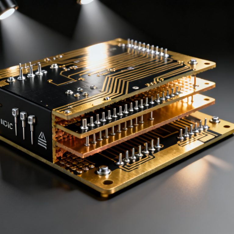
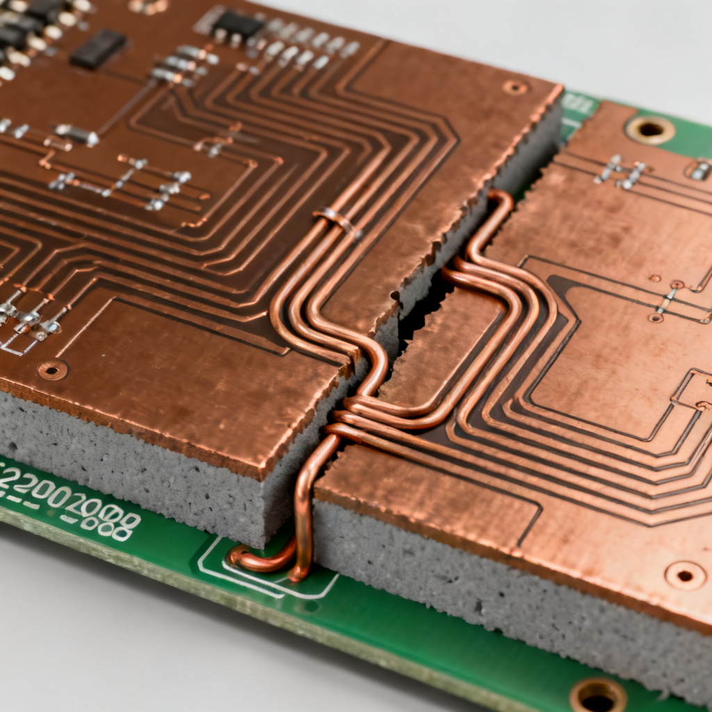
During layer transitions, the PCB return path must jump between planes. Place a ground via within 0.5 mm of every signal via to provide a low-inductance path for the return current.
Via Inductance: The Parasitic Enemy in High-Speed Design
What is Via Inductance?
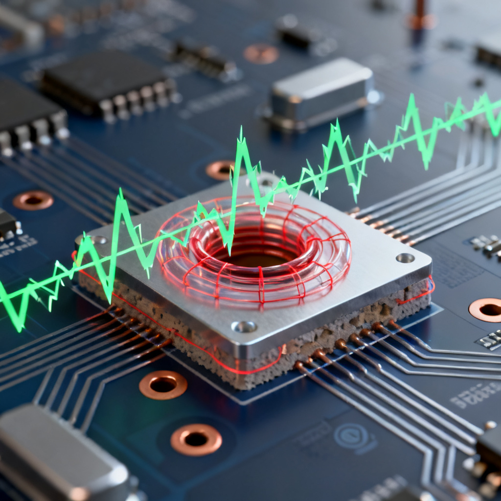
Via inductance is a parasitic effect proportional to via length and inversely proportional to diameter. A tall, thin via has high inductance that degrades signal and power integrity.
How Via Inductance Hurts Your Design
High via inductance creates impedance discontinuities, signal reflections, and poor power delivery. For high-speed signals above 1 Gbps, controlling via inductance is mandatory.
Rules to Minimize Via Inductance
- Shorten the via: Use thinner board stacks and route on surface layers.
- Increase via diameter: Use 0.5–1.0 mm vias for power connections.
- Use multiple vias in parallel: Two vias reduce inductance by ~50%; four vias by ~75%.
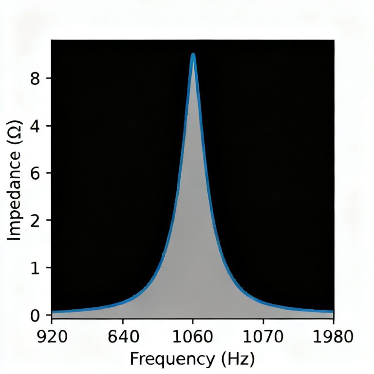
- Avoid via stubs: Use back-drilling or blind/buried vias for signals above 5 Gbps.
- Optimize pad and anti-pad: Balance capacitance and inductance for high-speed performance.
Power Integrity: Vias and Decoupling Capacitors
Minimize loop inductance between decoupling capacitors and vias. Place vias within 0.5 mm of capacitor pads and use two vias per capacitor for optimal power delivery.
Practical High-Speed Layout Rules: The Checklist
Routing and PCB Return Path Rules
Never route over a plane split. Keep high-speed traces close to their reference plane. For differential pairs, maintain symmetry and use a solid ground plane underneath.
Via Usage Rules
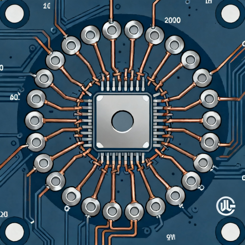
One ground via per signal via at layer transitions. Use multiple ground vias around connectors and ICs. For signals above 1 Gbps, use back-drilled or blind/buried vias to eliminate stubs.
Stitching and Shielding
Place ground vias around the PCB perimeter every 1/10th of the highest frequency wavelength. Use via fences along RF traces to isolate signals.
Common Mistakes and How to Fix Them
| Mistake | Symptom | Fix |
|---|---|---|
| Signal crossing a split plane | High EMI, signal glitches | Reroute over solid plane; use a stitching capacitor |
| Single via for a high-speed signal | Reflections, jitter | Add a ground via near the signal via |
| Tall, thin vias for power | Poor decoupling at high freq | Use shorter, wider vias; use multiple vias |
| No via stubs removal | Notch in frequency response | Back-drill or use blind/buried vias |
| Isolated ground pour | Acts as an antenna | Stitch the pour with vias to main ground plane |
FAQ: PCB Return Path and Via Inductance
What is a PCB return path and why is it important?
The PCB return path is the route high-frequency current takes back to its source. It is critical for signal integrity because a disrupted return path increases loop inductance and causes EMI.
How does via inductance affect high-speed signals?
Via inductance creates impedance discontinuities that reflect signals, slow edge rates, and degrade eye diagrams. Minimizing via inductance is essential for signals above 1 Gbps.
What is the best way to minimize via inductance?
Use short, wide vias; place multiple vias in parallel; and eliminate via stubs through back-drilling or blind/buried vias for optimal PCB return path performance.
How many ground vias are needed per signal via?
At least one ground via per signal via at layer transitions, placed within 0.5 mm, to maintain a low-inductance PCB return path.
What is back-drilling and when should I use it?
Back-drilling removes the unused via stub to prevent resonance. It is recommended for all high-speed signals above 5 Gbps to preserve signal integrity.
Conclusion: The Two Golden Rules
Return Path Rule: Always provide a continuous, low-inductance PCB return path directly under every high-speed signal trace. Via Inductance Rule: Treat every via as a parasitic inductor—keep vias short, wide, and multiple in parallel; for high-speed signals, eliminate via stubs.
See more about PCB Principles & Fundamentals.
Need expert PCB fabrication and assembly? We specialize in high-speed, multi-layer boards with back-drilling, blind/buried vias, and controlled impedance. Contact us for a quote.