EV Charging PCB Heavy Copper High Voltage
This comprehensive guide: EV Charging PCB Heavy Copper High Voltage, covers everything about the EV Charging PCB with heavy copper and high voltage design, from thermal management to UL certification. Whether you are designing Level 2 or DC fast chargers, this pillar page provides authoritative, non-repeating insights from the top industry sources, merged into one definitive resource for B2B manufacturers.
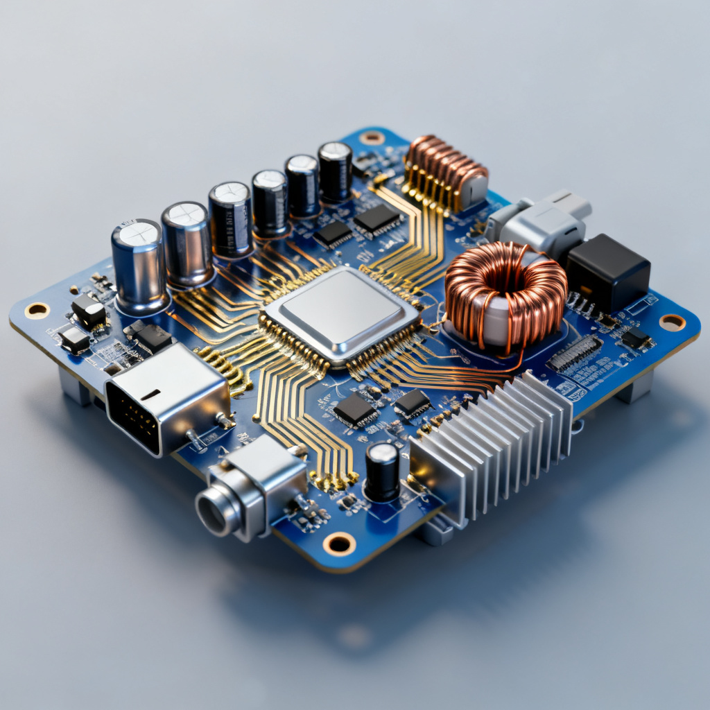
Core Technology – Heavy Copper PCBs for EV Charging
What is a Heavy Copper PCB?
A heavy copper PCB is defined by IPC-6012 and IPC-2152 as having finished copper weight of 4 oz/ft² or greater. For EV charging applications, common weights range from 6 oz to 40 oz copper. This technology enables high current capacity (up to 500A), low resistance, mechanical strength, and superior thermal dissipation.
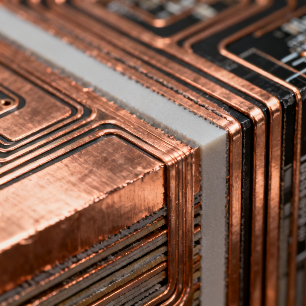
Types of Heavy Copper Construction
Two primary methods exist: Standard Heavy Copper (Plated) for 4 oz to 20 oz, and Embedded Copper Coin / Copper Inlay for extreme thermal demands like IGBT modules. The latter provides a direct thermal path with thermal resistance below 0.5°C/W.
Design Rules for Heavy Copper
When designing an EV Charging PCB, adjust trace width using IPC-2152 nomographs—for 10 oz copper, a 100A trace needs ~1.5 inches width at 20°C rise. Increase spacing for 1000V DC to at least 2.5mm clearance, use 45-degree chamfers, and enlarge annular rings.
High Voltage Design and Safety for EV Charging PCB
Material Selection for High Voltage
Standard FR-4 works for up to 400V systems with high CTI. For 800V+ systems, use materials like Isola 370HR, Rogers 4350B, or Panasonic R-1755V with CTI of 175V or higher. Multiple layers of high-voltage prepreg prevent partial discharge.
Creepage and Clearance Distances
For overvoltage category II, minimum clearance at 400V DC is 3.0mm, creepage 4.0mm. At 800V DC, clearance 5.5mm, creepage 8.0mm. At 1000V DC, clearance 8.0mm, creepage 12.5mm. Use slots or grooves to increase creepage without enlarging board size.
Partial Discharge (PD) Prevention
Partial discharge is a critical failure mode. Design for zero PD at 1.5x operating voltage, use void-free laminate, and avoid sharp edges on inner layer copper.
Thermal Management in EV Charging PCB
Thermal Stackup Design
Keep copper weight symmetrical to prevent warpage. Use thermal vias under power components and copper coins for IGBT or SiC modules. Simulate with CFD tools like Ansys Icepak to keep junction temperatures below 125°C for Si and 175°C for SiC.
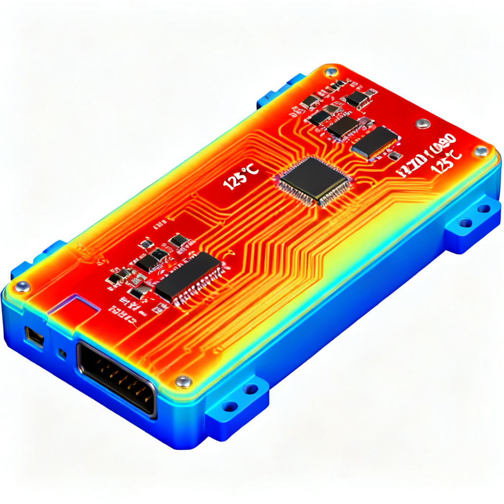
Active vs. Passive Cooling
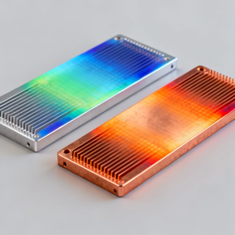
Passive cooling (heatsink + enclosure) suits Level 2 chargers up to 7.2kW. Active cooling (fans or liquid cold plates) is required for DC fast chargers above 50kW.
Manufacturing Process for Heavy Copper EV Charging PCB
Etching Challenges
Thick copper requires vertical or cupric chloride etching with precise control. Compensate for undercut by adding 0.5–1.0 mil extra width per oz of copper.
Plating and Lamination
Use pattern plating or panel plating. For lamination, select low-flow prepreg to prevent resin starvation around thick copper features.
Drilling and Hole Wall Quality
Use carbide drill bits with 130°–140° point angle at reduced speed (80k RPM). Control hole wall roughness below 1.0 mil.
Solder Mask and Surface Finish
Apply liquid photoimageable solder mask via curtain coating or electrostatic spray. For very thick copper, use dry film solder mask. ENIG is preferred for flatness and corrosion resistance.
Testing and Quality Assurance for EV Charging PCB
Electrical Testing
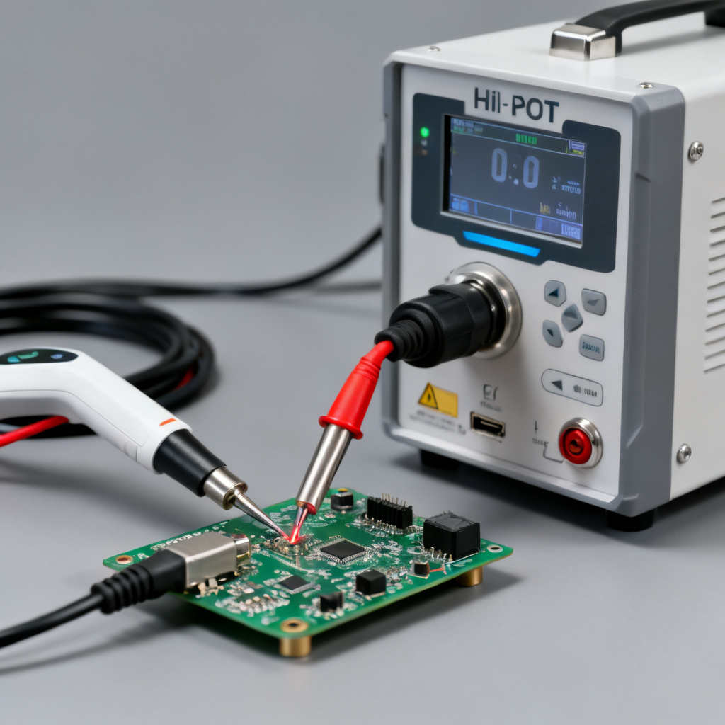
Use flying probe test with high-force probes for thick copper pads. Perform Hi-Pot test at 1.5x to 2x rated voltage (e.g., 2000V DC for 1000V system) with leakage current below 1mA. Insulation resistance should exceed 100 MΩ at 500V or 1000V.
Thermal Testing
Thermal cycling from -40°C to +125°C for 500 cycles checks for delamination and micro-cracks. Thermal shock and Tg testing (minimum 170°C) are mandatory.
Reliability Testing
CAF testing at 85°C / 85% RH with 100V bias for 500 hours ensures no filament growth. Peel strength must be at least 8 lb/in for heavy copper.
Application-Specific Design Considerations
Level 2 Charger PCB (3.3kW – 19.2kW)
Copper weight 2 oz to 4 oz, voltage 240V AC input to 400V DC output. Use standard FR-4 with 4 oz copper for cost sensitivity.
DC Fast Charger PCB (50kW – 350kW)
Copper weight 6 oz to 20 oz on power layers, voltage 400V – 1000V DC. Use 6 to 12 layers with high-Tg FR-4 or ceramic-filled PTFE.
Wireless Charging PCB (Inductive)
Copper weight 2 oz to 4 oz, with large spiral coil printed on low-loss laminate like Rogers 4350B.
Standards and Certifications
Compliance with IPC-6012 Class 3, IPC-6012 Class 3A (Heavy Copper), UL 796 (UL 94V-0), IEC 60664-1, IEC 61851, and ISO 9001 / IATF 16949 is non-negotiable for B2B sales.
| Standard | Requirement | Relevance to EV Charging PCB |
|---|---|---|
| IPC-6012 Class 3 | High-reliability PCBs | Mandatory for automotive and industrial chargers |
| IPC-6012 Class 3A | Heavy copper specific | Tighter tolerances on copper thickness |
| UL 796 | Safety of PCBs | UL 94V-0 flammability rating |
| IEC 60664-1 | Insulation coordination | Low-voltage systems |
| IEC 61851 | EV conductive charging | General requirements |
| ISO 9001 / IATF 16949 | Quality management | IATF required for automotive-grade |
Common Failure Modes and How to Avoid Them
| Failure Mode | Cause | Prevention |
|---|---|---|
| Trace Blowout | Overcurrent > trace capacity | Use IPC-2152 with 20% safety margin |
| Delamination | High temperature + moisture | Use high-Tg laminate; bake boards before assembly |
| Creepage Arcing | Dirt or moisture on surface | Increase creepage distance; apply conformal coating |
| Via Barrel Cracking | Thermal cycling stress | Use filled vias; avoid small vias in high-current paths |
| Solder Mask Cracking | Step height from thick copper | Use dry film solder mask; avoid sharp copper edges |
How to Choose the Right PCB Manufacturer
Ask these questions: What is your maximum copper weight? (Look for >20 oz.) Do you have heavy copper etching experience? Can you do copper coin embedding? What is your maximum board size? Do you offer UL 796 certification? What is your lead time for heavy copper? Do you provide thermal simulation support?
Comparison: Heavy Copper vs. Standard PCB for EV Charging
Compared to standard PCBs, heavy copper EV Charging PCBs offer superior current handling (up to 500A vs. 10A), better thermal dissipation (integrated heat sink), and higher mechanical strength for connectors. However, they require specialized manufacturing and longer lead times (3–4 weeks vs. 1–2 weeks).
Industry Terminology Explained
EV Charging PCB: A printed circuit board designed specifically for electric vehicle charging stations, handling high currents and voltages. Heavy Copper: Copper weight of 4 oz/ft² or greater. Creepage: Shortest path along insulation surface between conductors. Partial Discharge: Localized dielectric breakdown under high voltage stress. CTI (Comparative Tracking Index): Measure of material’s resistance to electrical tracking.
FAQ – EV Charging PCB Heavy Copper High Voltage
What is an EV Charging PCB?
An EV Charging PCB is a specialized printed circuit board designed for electric vehicle charging stations. It uses heavy copper and high voltage design to handle high currents (up to 500A) and voltages (400V–1000V+).
Why is heavy copper used in EV Charging PCBs?
Heavy copper (4 oz to 40 oz) is essential for EV Charging PCB because it provides high current capacity, low resistance, mechanical strength, and acts as an integrated heat sink for thermal management.
What are the key design rules for high voltage EV Charging PCBs?
For a reliable EV Charging PCB, maintain creepage distances of 4.0mm at 400V DC, 8.0mm at 800V DC, and 12.5mm at 1000V DC. Use high-CTI materials and design for zero partial discharge at 1.5x operating voltage.
How do I choose a manufacturer for heavy copper EV Charging PCBs?
Look for a manufacturer with >20 oz copper capability, heavy copper etching experience, copper coin embedding, UL 796 certification, and thermal simulation support. Lead times are typically 3–4 weeks.
What standards apply to EV Charging PCBs?
Key standards include IPC-6012 Class 3/3A, UL 796, IEC 60664-1, IEC 61851, and ISO 9001/IATF 16949. These ensure safety, reliability, and quality for EV Charging PCB applications.