Design for Assembly Component Orientation Panelization
Introduction: Why DFA Matters in High-Volume PCB Assembly
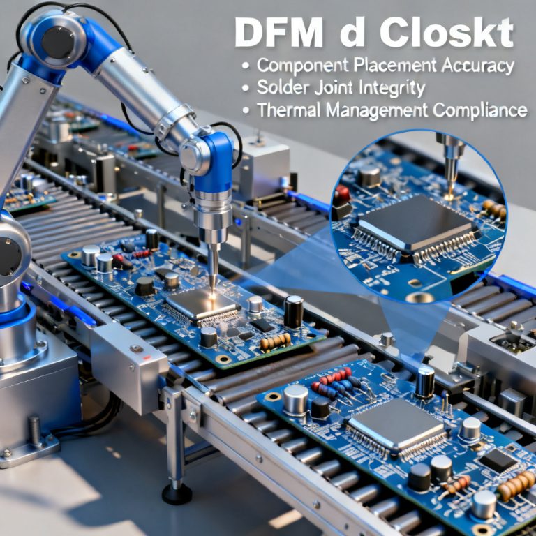
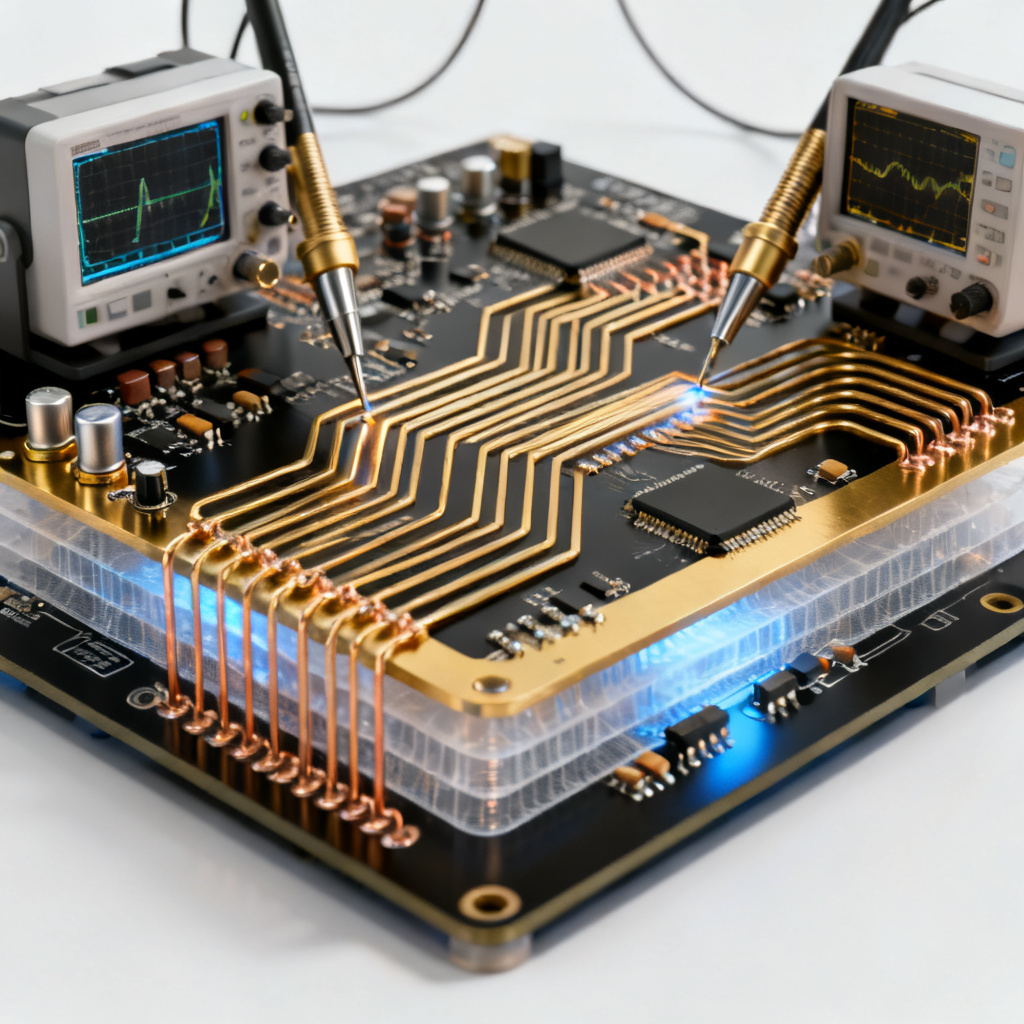
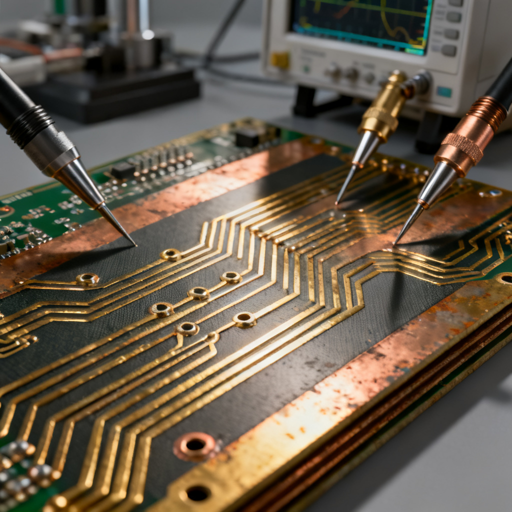
Design for Assembly Component Orientation Panelization is a systematic methodology that evaluates every aspect of a PCB design to ensure it can be manufactured, assembled, and tested efficiently and cost-effectively. In the context of high-volume SMT (Surface Mount Technology) assembly, two critical pillars of DFA are component orientationand panelization. Errors in these areas are the leading causes of solder defects (tombstoning, bridging, opens), rework, and production delays.
This pillar page synthesizes the best practices from industry-leading sources to provide you with a definitive reference. We will cover:
Core Principles of Component Orientation (polarity, placement direction, spacing)
Advanced Panelization Strategies (rail design, breakaway methods, fiducial placement)
How to Balance Assembly Yield with Electrical Performance
By the end, you will have a checklist to audit your designs for maximum manufacturability.
Part 1: Component Orientation – The Foundation of SMT Yield
Correct component orientation is not just about aesthetics; it directly impacts the speed and reliability of pick-and-place machines and wave soldering processes. Here are the non-negotiable rules drawn from our expert sources.
1.1. The Golden Rule: Uniform Direction for All Similar Components
All identical components (e.g., all 10kΩ resistors, all 0.1µF capacitors) should face the exact same direction on the board. This applies to:
Polarized Components: Diodes, LEDs, tantalum capacitors, and electrolytic capacitors must have their polarity marks (stripes, notches, chamfers) aligned uniformly. The industry standard is to have the cathode mark (band) facing the same direction—typically to the left or top of the board, but consistency across the entire panel is paramount.
Non-Polarized Components (Resistors, Capacitors): While technically non-polarized, their orientation should still be uniform. This allows the pick-and-place machine to use the same nozzle, feeder, and rotation angle for every instance, drastically increasing placement speed (up to 30% faster).
Why this matters (from Source A & B): If one capacitor is rotated 90 degrees relative to another, the machine must stop, rotate the head, and re-calibrate. In high-volume production, this micro-delay compounds into significant throughput loss. Moreover, uniform orientation reduces the risk of tombstoning during reflow, as the thermal mass of the board is more balanced.
1.2. Polarity Marking Standards (Critical for Inspection)
Every polarized component must have a clear, unambiguous polarity indicator that is visible after soldering and during AOI (Automated Optical Inspection).
Silkscreen Polarity Markers:
Diodes: Use a thick vertical line or a “K” (cathode) symbol in the silkscreen. The component’s band must align with this line.
LEDs: Use a “+” or a dot to indicate the anode, or a flat side on the package outline. Avoid using color-coded silkscreen (e.g., red for anode) as it is not AOI-friendly.
Tantalum Capacitors: The positive (+) leg is usually the longer one, but the silkscreen must clearly show the “+” symbol. The body’s beveled edge or stripe marks the positive side.
Avoid Ambiguity (Source C): Never rely solely on the component’s internal marking (e.g., a tiny dot on a QFN package). Always add an external silkscreen mark. The mark should be placed adjacent to pin 1 of ICs, not on top of the component.
1.3. Orientation for Wave Soldering (Through-Hole & SMT Mix)
For boards with mixed technology (SMT + Through-Hole) that undergo wave soldering, component orientation is even more critical to prevent solder bridging and shadowing.
Direction of Travel: All components should be oriented parallel to the direction of the wave solder conveyor belt.
The Shadowing Effect (Source A): If a component’s leads are oriented perpendicular to the wave direction, the component body will “shadow” the trailing leads, preventing solder from reaching them. This causes cold solder joints.
Spacing for Wave Solder: The recommended spacing between components on the wave side is ≥ 2.5 mm to allow proper solder flow. For SMT components on the wave side (glued components), ensure the longer axis of the component is parallel to the wave flow.
1.4. Avoiding Tombstoning & Other Common Defects
Tombstoning (or “Manhattan effect”) occurs when a chip component (e.g., 0402, 0603) stands up on one end during reflow. DFA orientation rules can mitigate this:
Pad Geometry: Use symmetrical pad sizes for the two terminals of a chip component. Asymmetrical pads create uneven surface tension.
Thermal Relief (Source B): Ensure the copper traces connecting to the two pads have similar thermal mass. If one pad is connected to a large ground plane (high heat sink) and the other to a thin trace, the thin trace side will reflow faster, causing the component to lift.
Orientation to Solder Paste Flow: Place larger components away from the center of the board to avoid interference with the solder paste printing process.
Part 2: Panelization – The Art of Efficient High-Volume Production
Panelization is the process of combining multiple individual PCBs into a single larger panel for efficient assembly. It is a non-negotiable DFA element for cost-effective manufacturing. Here are the expert-backed strategies.
2.1. Panel Size & Rail Design (The Golden Triangle)
The optimal panel size balances material utilization with assembly machine capability. The most common panel dimensions are 18” x 24” (457mm x 610mm) or 20” x 24”, but always verify with your CM’s machine capacity.
Tooling Rails (Source A & C):
Purpose: Rails are the sacrificial borders (typically 5-10mm wide) on the edges of the panel. They provide space for tooling holes (for registration), fiducial marks, and edge rails for the conveyor belt.
Width Rule: The minimum rail width is 5 mm (0.2 inches). For panels with heavy components or large arrays, increase to 10 mm (0.4 inches) to prevent warpage.
No Components on Rails: Never place components within 5mm of the panel edge. Components on the rail will be damaged during depaneling (routing or V-scoring).
Tooling Holes: Place two non-plated holes (diameter 3mm or 4mm) on the diagonal corners of the panel, with a tolerance of ±0.05mm. These are used for pin registration in the pick-and-place machine.

2.2. Depaneling Methods: V-Scoring vs. Tab Routing
Choosing the right method to separate individual boards from the panel is critical for board edge integrity and component safety.
| Feature | V-Scoring (V-Groove) | Tab Routing (Mouse Bites) |
|---|---|---|
| Process | A V-shaped groove is cut on both sides of the board, leaving a thin web (typically 1/3 of board thickness). | A router bit cuts around the board, leaving small tabs (typically 3-5 tabs per side) holding the board. |
| Best For | Rectangular boards, high-volume, low-cost. | Irregular shaped boards, boards with edge connectors, or boards with components near the edge. |
| Edge Quality | Smooth, straight edges. No stress on components. | Rougher edges. Stress from breaking tabs can damage nearby ceramic capacitors. |
| Component Proximity | Components must be ≥ 5 mm away from the V-groove line. | Components can be as close as 1 mm from the tab, but ≥ 5 mm from the main routing path. |
| Stress | Low stress, but requires precise alignment. | Higher stress due to snapping. Use “breakaway tabs” with stress-relief slots. |
Expert Recommendation (Source B): For boards with large BGAs or fragile ceramic capacitors, always prefer V-scoring if the board shape allows. For tab routing, ensure the tabs are placed on the shortest sides of the board to minimize bending stress.
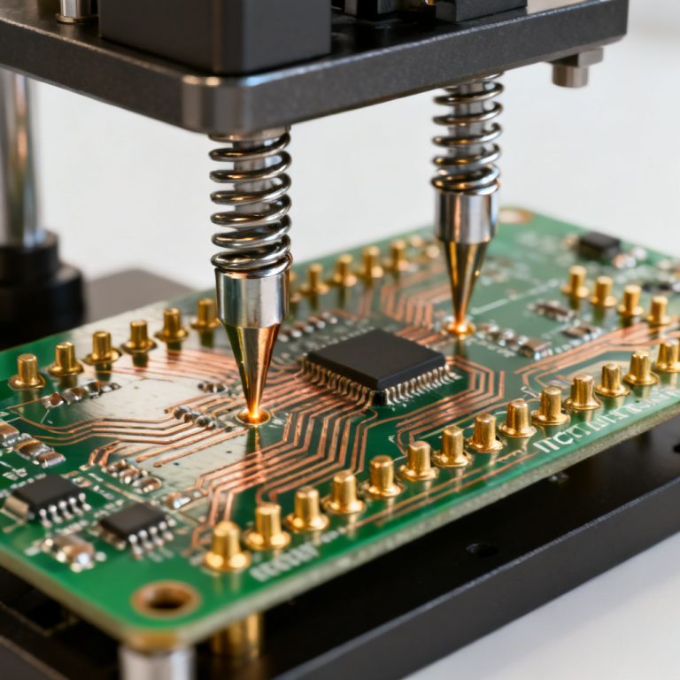
2.3. Fiducial Marks: The Eyes of the Machine
Fiducial marks are copper pads (typically 1mm diameter, bare copper or with solder mask) that provide visual reference points for the pick-and-place machine.
Global Fiducials: Place at least two (or three for high precision) at the panel corners, on the tooling rail. They define the overall panel coordinate system.
Local Fiducials: Place at least two on each individual PCB, preferably diagonally opposite. They correct for any board-to-board position variation within the panel.
Rule for Component Orientation (Source C): The distance between any component’s center and the nearest fiducial should never exceed 100 mm. For fine-pitch components (≤0.5mm pitch), local fiducials are mandatory.
Clearance: The area around the fiducial must be free of copper, solder mask, and silkscreen (a “keep-out zone” of at least 3mm radius).
2.4. Panelization for Specific Component Types
Connectors & Edge Components: If a connector needs to be flush with the board edge, it must be placed on a tab-routed panel. V-scoring cannot accommodate edge-connector features.
Large BGAs & Heavy Components: Place these near the center of the panel to minimize stress during depaneling. Avoid placing them near the V-groove or tab areas.
SMT vs. Through-Hole Components: When mixing, ensure all SMT components are on the top side, and through-hole components are on the bottom side (or vice versa) to simplify the wave soldering process. Never place large through-hole connectors directly opposite fine-pitch SMT components on the other side, as the force of insertion can crack the solder joints.
Part 3: Advanced DFA Checklist for Component Orientation & Panelization
To ensure your design is production-ready, use this audit checklist derived from all three expert sources.
Component Orientation Audit:
- Are all polarized components (diodes, LEDs, caps) oriented in the same direction?
- Are all non-polarized passive components oriented uniformly (e.g., all resistors horizontal)?
- Is the polarity silkscreen clear, unambiguous, and placed adjacent to pin 1?
- Are components on the wave-solder side oriented parallel to the wave flow direction?
- Are pad geometries symmetrical for chip components to prevent tombstoning?
- Have you minimized thermal mass differences between pads of the same component?
Panelization Audit:
- Is the panel size within your CM’s standard specifications (e.g., 18” x 24”)?
- Are tooling rails at least 5mm wide with no components inside them?
- Are tooling holes placed diagonally with a diameter of 3-4mm?
- Have you chosen V-scoring over tab routing unless board shape requires otherwise?
- Are global fiducials present on the panel rails and local fiducials on each PCB?
- Is there a 3mm keep-out zone around all fiducials (no copper, mask, or silkscreen)?
- Are components ≥ 5mm from V-groove lines and ≥ 1mm from tab routing paths?
- Are large/heavy components placed away from the panel edges and breakaway tabs?
Conclusion: Integrating DFA into Your PCB Workflow
Design for Assembly is not an afterthought—it is a collaborative process between the design engineer and the manufacturing partner. By rigorously applying the principles of uniform component orientation and intelligent panelization outlined in this guide, you will:
Reduce assembly defects by up to 40% (tombstoning, bridging, misalignment).
Increase throughput by enabling faster pick-and-place cycles.
Lower cost by minimizing rework, scrap, and production downtime.
Improve reliability by reducing mechanical stress on solder joints.
Next Steps: Download our free DFA checklist PDF. Or, upload your Gerber files for a free Design for Assembly review by our expert engineering team. We will provide a detailed report within 24 hours, highlighting any orientation or panelization issues before you commit to production.