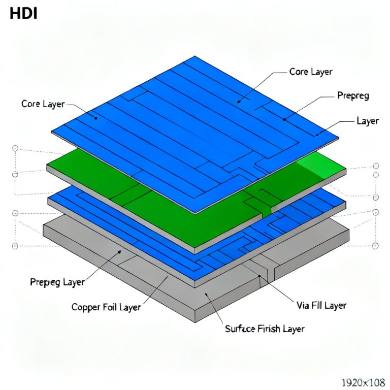
Test Method Comparison ICT vs Flying Probe AOI vs AXI
In B2B PCB manufacturing, mastering the Test Method Comparison – ICT vs Flying Probe, AOI vs AXI is essential for zero-defect production and export success. This guide explores each technique’s strengths, costs, and ideal use cases, drawing from top industry sources to help you choose the right inspection strategy.

1. Electrical Testing: ICT vs Flying Probe
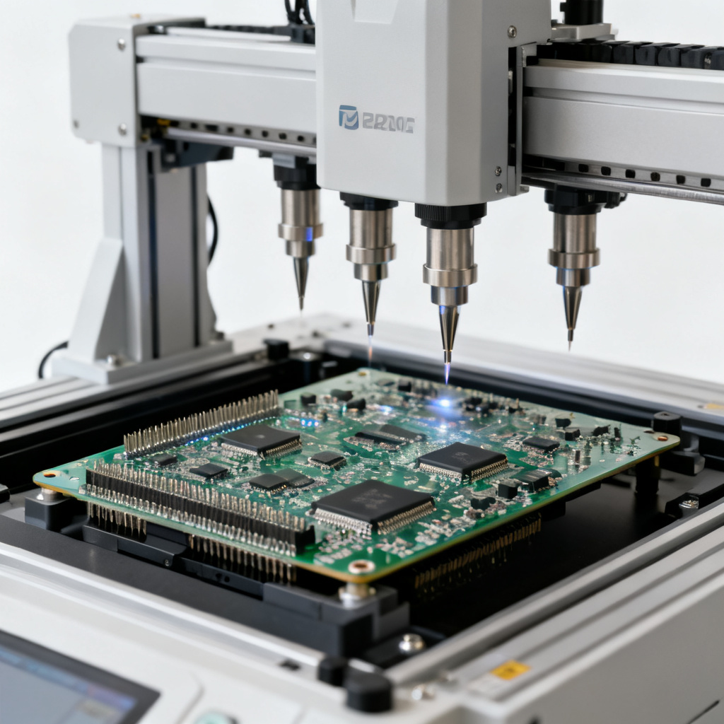
In-Circuit Test (ICT) – High-Volume Workhorse
The Test Method Comparison – ICT vs Flying Probe, AOI vs AXI begins with ICT, a bed-of-nails fixture test that contacts every net simultaneously. ICT is extremely fast (1–5 seconds per board), making it ideal for high-volume production (10,000+ units). It detects shorts, opens, and component values with high accuracy, but requires a custom fixture costing $1,000–$5,000+. This method is best for mature designs where NRE amortizes over large batches. However, ICT cannot test fine-pitch components like BGA without dedicated test points.
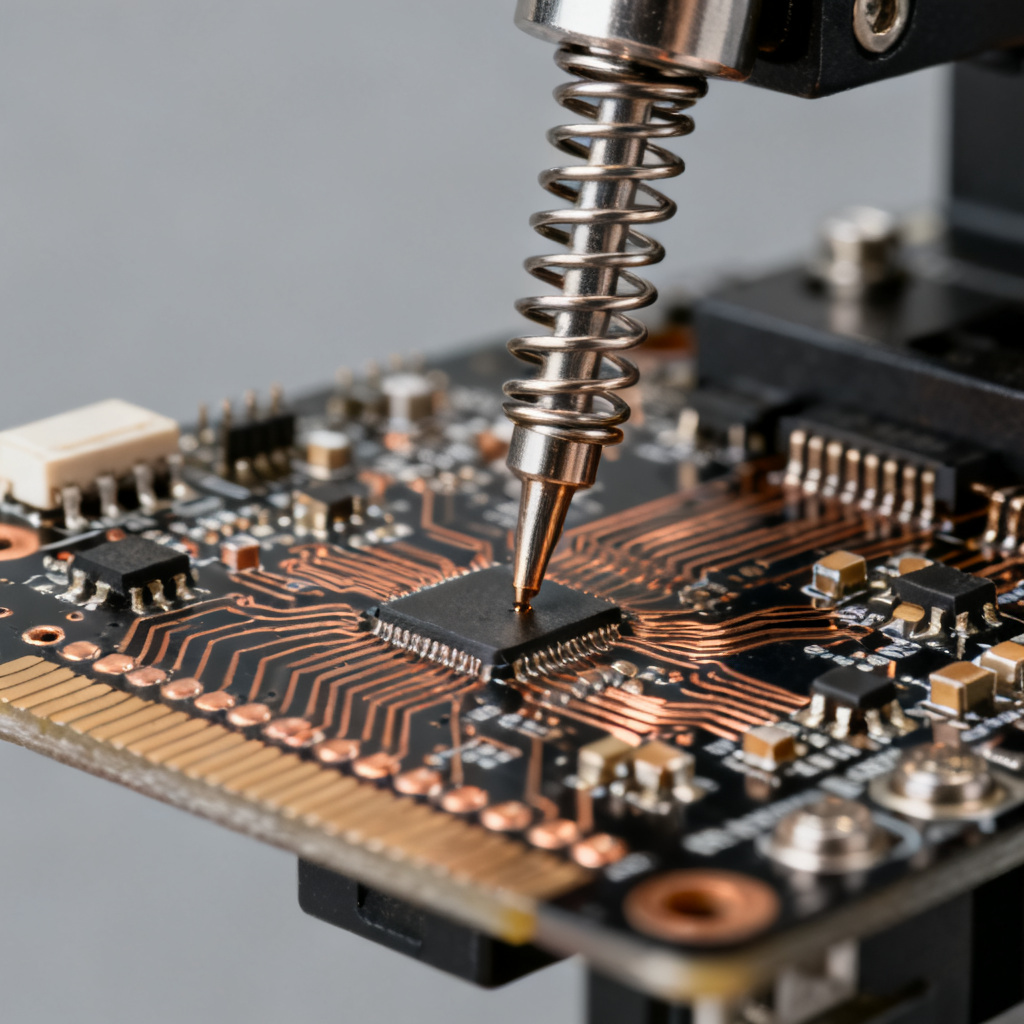
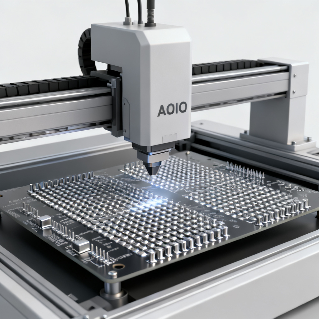
Flying Probe – Fixtureless Flexibility
Flying probe testing uses moving probes to contact test points sequentially, eliminating fixture costs. In the Test Method Comparison – ICT vs Flying Probe, AOI vs AXI, flying probe is slower (1–10 minutes per board) but offers zero NRE, making it perfect for prototypes and low-volume runs (1–1,000 units). It excels with complex, fine-pitch designs but struggles with high-frequency traces and cannot test BGA unless test points are provided. Modern machines can test active components like diodes, but coverage is less comprehensive than ICT.
2. Visual Inspection: AOI vs AXI
Automated Optical Inspection (AOI) – Surface-Level Precision
AOI uses high-resolution cameras to detect surface defects like missing components, polarity errors, and solder bridges. In the Test Method Comparison – ICT vs Flying Probe, AOI vs AXI, AOI is fast (10–30 seconds per board) and cost-effective, but it cannot see under components (e.g., BGA). 3D AOI measures solder joint height, improving detection of head-in-pillow defects. It is a first-pass quality gate for visible joints.
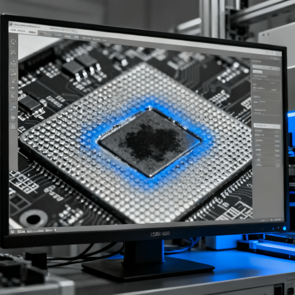
Automated X-Ray Inspection (AXI) – Hidden Joint Mastery
AXI penetrates the PCB to inspect internal structures, including BGA, QFN, and vias. In the Test Method Comparison – ICT vs Flying Probe, AOI vs AXI, AXI is slower (30 seconds to 2 minutes per board) and more expensive, but it is essential for high-reliability applications (aerospace, medical, automotive). It detects voids, cracks, and internal shorts that AOI misses. 3D CT scanning provides layer-by-layer analysis for complex assemblies.
3. Structured Comparison Tables
| Feature | ICT (In-Circuit Test) | Flying Probe |
|---|---|---|
| Speed | Very Fast (1–5 sec/board) | Slow (1–10 min/board) |
| Fixture Cost | High ($1k–$5k+) | None |
| Volume Suitability | High Volume (10k+) | Low-Medium Volume (1–1000) |
| Test Coverage | Comprehensive | Good (shorts, opens, passives) |
| Fine-Pitch Support | Limited | Better |
| Feature | AOI | AXI |
|---|---|---|
| Technology | Visible light cameras | X-ray radiation |
| What It Sees | Surface-level defects | Internal & hidden structures |
| Speed | Fast (10–30 sec/board) | Slower (30 sec–2 min/board) |
| Hidden Joints (BGA) | Cannot detect | Essential for detection |
| Internal Voids/Cracks | Cannot detect | Can detect |
4. Integrated Testing Strategy
The Test Method Comparison ICT vs Flying Probe AOI vs AXI reveals that no single method is sufficient. Top manufacturers layer tests: First, AOI post-paste and post-reflow to catch surface defects. Second, AXI for hidden BGA/QFN joints. Third, electrical testing (ICT for high volume, flying probe for low volume). For high-volume BGA boards: Solder Paste AOI → Pick & Place → Reflow → Post-Reflow AOI → Post-Reflow AXI → ICT → Functional Test. For low-volume fine-pitch boards: Solder Paste AOI → Reflow → Post-Reflow AOI → Flying Probe → AXI spot check.