Mechanical Parameters Thickness Warpage Hole Tolerance
Understanding Mechanical Parameters – Thickness, Warpage, Hole Tolerance is essential for reliable PCB fabrication and assembly. These three physical dimensions determine board fit, solder joint quality, and long-term performance in demanding applications like automotive, aerospace, and high-speed digital systems.
1. PCB Thickness: The Foundation of Mechanical Integrity
PCB thickness directly impacts mechanical strength, thermal management, impedance control, and enclosure compatibility. The most common finished board thickness is 1.6mm (0.062 inches), but this varies with layer count, copper weight, and application.
Standard Thickness Ranges and Tolerances for Mechanical Parameters
| Board Type | Typical Thickness Range | Standard Tolerance (IPC-6012 Class 2) |
|---|---|---|
| 2-4 layer standard | 0.8mm – 2.4mm | ±10% (e.g., 1.6mm ±0.16mm) |
| 6-10 layer high-density | 1.6mm – 2.0mm | ±10% |
| 20+ layer complex | 2.0mm – 3.2mm | ±10% |
| Flex / rigid-flex | 0.1mm – 0.3mm (flex section) | ±0.05mm |
| Heavy copper (2oz-10oz) | 1.8mm – 2.5mm | ±10% |
Mechanical Parameters – Thickness, Warpage, Hole Tolerance are interrelated: a board that is too thin may warp more easily, while tight hole tolerances require adequate core thickness for drilling stability. Always specify finished board thickness (including copper and solder mask) with a realistic tolerance.
How Thickness is Achieved and Measured
Final thickness is the sum of core, prepreg, and copper foil. Nominal thickness tolerance is typically ±10% for standard boards. High-precision applications (aerospace, medical) may require ±0.1mm or even ±0.05mm. Key factors affecting consistency include prepreg resin content, copper distribution, and lamination pressure/temperature.
Why Thickness Matters for Mechanical Parameters
- Mechanical fit: A board too thick won’t fit enclosures; too thin flexes excessively, causing solder joint stress.
- Impedance control: Dielectric thickness must be tightly controlled for controlled impedance designs.
- Thermal management: Thicker boards dissipate heat better but create thermal gradients during soldering.
- Vibration/shock resistance: Thicker, stiffer boards perform better in harsh environments.
Industry Standards and Best Practices
- IPC-6012 (Rigid PCBs): Defines thickness tolerances: Class 2 ±10%, Class 3 tighter.
- IPC-4101 (Prepreg and Core Materials): Specifies standard thickness ranges; designers should select from tables to avoid custom fabrication.
- Design for Manufacturing (DFM): Specify finished board thickness with realistic tolerance (±0.1mm achievable but may increase cost).
2. PCB Warpage: The Enemy of Assembly and Reliability
Warpage (bow and twist) is the deviation from a flat plane, quantified as maximum deflection divided by board diagonal length, expressed as a percentage. Even slight warp causes misalignment during component placement, soldering defects, and mechanical stress.
Causes of Warpage in Mechanical Parameters Context
- Uneven copper distribution: Heavy copper on one side, minimal on the other causes differential thermal expansion during lamination and reflow.
- Asymmetric layer stackup: Different copper weights or prepreg types on opposite sides create internal stresses.
- Thermal stress during soldering: Lead-free soldering (260°C peak) induces more stress than leaded processes.
- Material selection: Low-Tg FR-4 (130-140°C) softens more; high-Tg (170-180°C) and polyimide offer better dimensional stability.
- Panel size and aspect ratio: Larger panels warp more; square panels warp less than long, narrow ones.
- Core and prepreg cure: Incomplete curing creates residual stresses.
Acceptable Warpage Limits (Industry Standards)
| Technology | Maximum Warpage (IPC-6012) | Example (100mm diagonal) |
|---|---|---|
| Surface Mount (SMT) | 0.75% | 0.75mm deflection |
| Fine-pitch BGA (0.4mm pitch) | 0.5% | 0.5mm deflection |
| Through-Hole (THT) | 1.5% | 1.5mm deflection |
| Thick boards (>2.4mm) | Slightly higher limits | Per manufacturer |
Many high-volume manufacturers guarantee warp <0.5% for standard boards; complex high-layer-count boards typically achieve <0.75%.
How to Minimize Warpage: Design and Process Tips
- Symmetric stackup: Balance copper weight, prepreg type, and core thickness on both sides.
- Even copper distribution: Use copper pour (ground planes) on all layers; avoid large bare dielectric areas on one side.
- Use high-Tg materials: Specify FR-4 with Tg ≥170°C or polyimide for multiple reflow cycles.
- Reduce panel size: Break large panels into smaller arrays; use routing instead of V-scoring.
- Controlled lamination profile: Slow cool-down cycle reduces residual stresses.
- Post-lamination annealing: Stress-relief bake (150°C for 2-4 hours) after lamination.
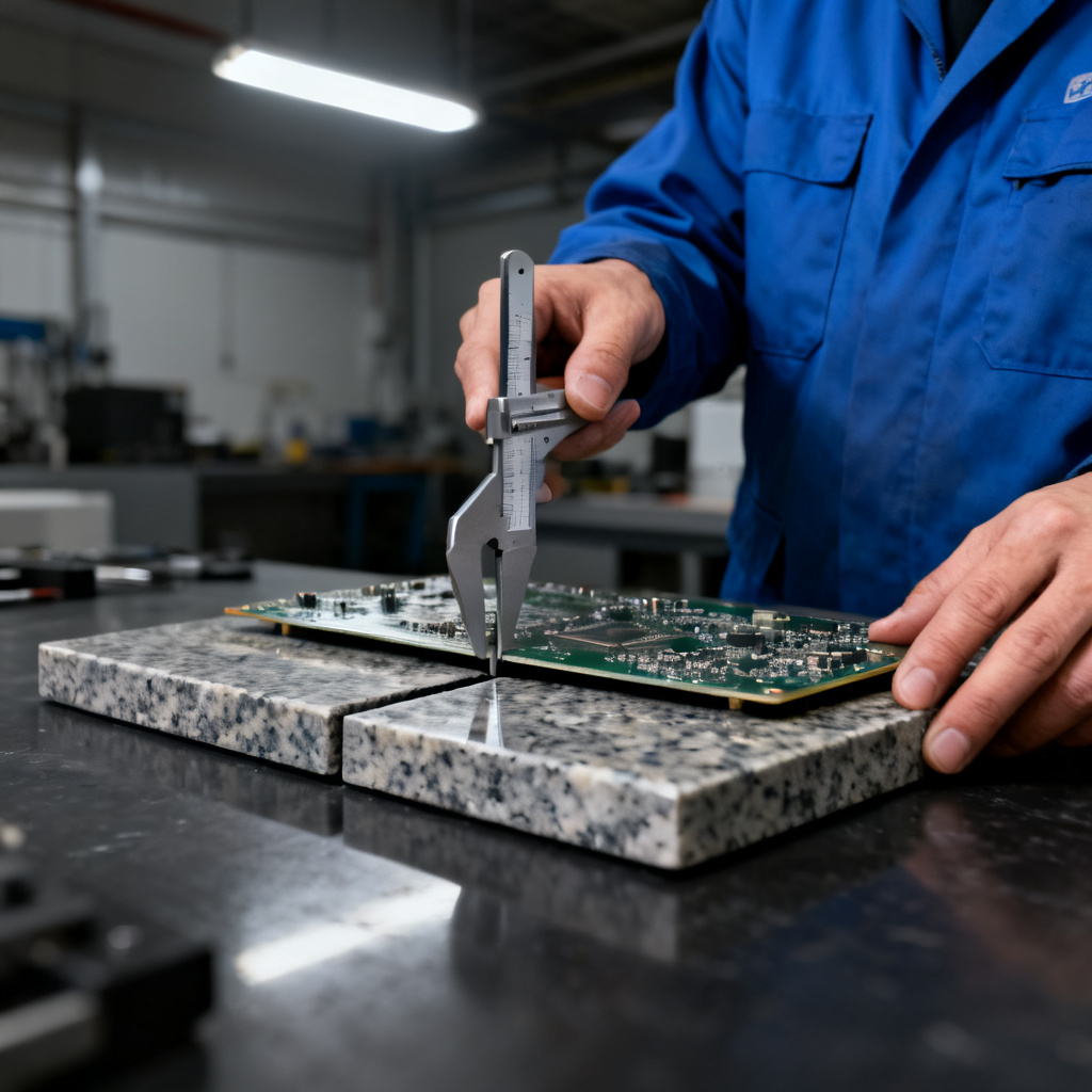
Measuring Warpage
Per IPC-TM-650 Method 2.4.22: board placed on flat surface, maximum gap measured. Warpage (%) = (Maximum Deflection / Diagonal Length) x 100. For a 200mm diagonal board with 1.2mm gap, warp is 0.6% (acceptable for SMT).
Warpage in Assembly: What to Watch For
- Stencil printing: Uneven solder paste deposition.
- Pick-and-place: Vacuum nozzles may misalign.
- Reflow soldering: Tombstoning, solder balling, insufficient joints.
- Inspection: AOI and X-ray false failures.
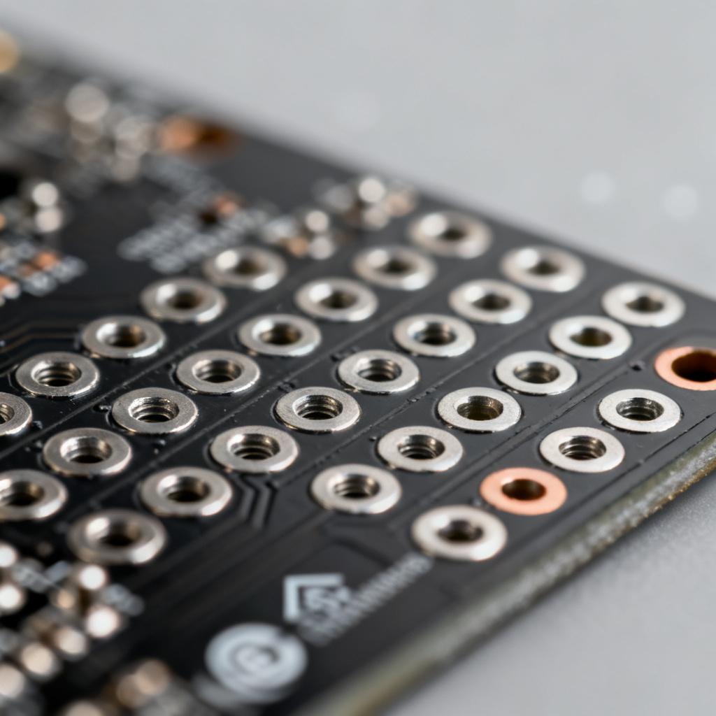
3. Hole Tolerance: Precision for Reliable Interconnections
Hole tolerance is the allowable variation in drilled hole diameter (plated through-holes, vias, mounting holes). It directly affects component lead insertion, solder joint quality, and electrical connectivity. Mechanical Parameters – Thickness, Warpage, Hole Tolerance must be considered together: a board with tight hole tolerances may require thicker core to maintain rigidity.
Types of Holes and Their Tolerances
| Hole Type | Typical Tolerance (Class 2) | Typical Tolerance (Class 3) |
|---|---|---|
| Plated Through-Hole (PTH) – standard | ±0.075mm to ±0.1mm | ±0.05mm |
| PTH – precision (<0.6mm) | ±0.05mm | ±0.025mm |
| Non-Plated Through-Hole (NPTH) | ±0.05mm to ±0.075mm | ±0.025mm |
| Microvias (HDI, <0.3mm) | ±0.025mm to ±0.05mm | ±0.025mm |
| Slot / elongated holes | ±0.1mm to ±0.15mm | ±0.1mm |
How Hole Tolerance is Determined
Drill bit wear, spindle runout, material swelling, and plating thickness all affect final hole diameter. For PTH, copper plating adds 0.025mm to 0.05mm per wall, reducing finished hole size. Manufacturers replace bits after 500-2000 hits; high-end machines have runout <0.01mm.
Industry Standards for Hole Tolerance
- IPC-6012 (Rigid PCBs): Class 2: ±0.075mm PTH, ±0.05mm NPTH. Class 3: ±0.05mm PTH, ±0.025mm NPTH.
- IPC-7351 (Component Footprints): Recommended hole sizes for different leads; e.g., 0.6mm lead needs 0.8mm-0.9mm finished hole.
Hole Tolerance and Component Fit
Annular ring: For 0.6mm finished hole, minimum annular ring is 0.15mm (Class 2) or 0.2mm (Class 3). Lead-to-hole clearance: Should be 0.15mm to 0.3mm. Press-fit holes: Tolerance ±0.025mm for reliable interference fit.
Design Tips for Hole Tolerance
- Use standard hole sizes: 0.3mm, 0.4mm, 0.6mm, 0.8mm, 1.0mm to avoid custom drill bits.
- Specify finished hole size (after plating) for PTH.
- Allow for plating thickness: Drilled hole may be 0.9mm-1.0mm for 0.8mm finished hole.
- Aspect ratio: Board thickness / hole diameter ≤10:1 for standard plating; ≤8:1 for high-reliability.
- Tolerance stack-up: Use positional tolerance (e.g., ±0.1mm for hole center) in addition to diameter tolerance.
Measuring Hole Tolerance
Go/No-Go gauges, pin gauges, optical measurement (for microvias), and ultrasonic methods (for plating thickness) are used.
Common Hole Tolerance Issues and Solutions
- Oversized holes: Worn drill bits or high runout. Solution: regular bit replacement, machine calibration.
- Undersized holes (PTH): Excessive plating or moisture absorption. Solution: control plating bath chemistry, pre-bake materials.
- Oval holes: Drill bit deflection or material movement. Solution: stiffer drill bits, optimized drilling parameters.
Conclusion: Integrating Mechanical Parameters into Your PCB Design
Mechanical Parameters Thickness Warpage Hole Tolerance,Thickness, warpage, and hole tolerance are not isolated—they interact with each other and the entire manufacturing process. By understanding IPC-6012, IPC-4101, and design principles (symmetric stackup, even copper distribution, standard hole sizes), you can specify reliable, cost-effective PCBs.
Key Takeaways:
- Specify finished board thickness with realistic tolerance (±10% standard, ±5% high-reliability).
- Design for minimal warpage: symmetric stackup, even copper, high-Tg materials for lead-free soldering.
- Use standard hole sizes; specify finished hole diameter for PTH; allow for plating thickness and tolerance.
- Communicate with your manufacturer early; provide detailed fabrication drawing including all mechanical parameters.
For complex or high-reliability projects, request a DFM review from your PCB supplier to identify potential warpage, thickness, or tolerance issues before production.