Solder Mask Application LPI Spray and Curtain
Solder mask application is a critical process in PCB manufacturing that determines board reliability, resolution, and cost. This guide Solder Mask Application LPI Spray and Curtaincovers three primary solder mask application methods—Liquid Photoimageable (LPI), Spray, and Curtain Coating—to help B2B buyers make informed decisions for custom PCB production and export.
1. Liquid Photoimageable (LPI) Solder Mask Application – High-Resolution Standard
1.1 What is LPI Solder Mask Application?
LPI solder mask application uses a two-component, photosensitive liquid epoxy or acrylic-based resin. The LPI solder mask application process involves applying the material to the entire board surface, selectively exposing it to UV light through a phototool, and chemically developing away uncured areas. This solder mask application method is the most widely adopted for high-volume, high-reliability PCBs due to excellent resolution and durability.
1.2 LPI Solder Mask Application Process
The LPI solder mask application process begins with surface preparation. The copper surface must be thoroughly cleaned and micro-etched to remove oxides and ensure strong adhesion. A chemical cleaning sequence typically includes alkaline cleaning, rinsing, and a micro-etch using sodium persulfate or sulfuric acid/hydrogen peroxide. After etching, the panel is rinsed with deionized water and dried in a convection oven.
LPI is applied by screen printing, curtain coating, or electrostatic spray during solder mask application. For standard LPI, screen printing is common. The mask is applied in a controlled thickness (typically 15–30 µm after final cure). For fine-pitch designs, vacuum lamination or electrostatic spray is preferred to ensure uniform coverage over tall traces and into tight spaces.
The wet mask is then placed in a low-temperature oven (70–80°C for 15–30 minutes) to evaporate solvents and partially cure the resin. A phototool is aligned with the panel, and the panel is exposed to high-intensity UV light (typically 350–400nm) for 300–600 mJ/cm². The exposed areas polymerize and become insoluble.
The panel is sprayed with a developer solution (dilute sodium carbonate or potassium carbonate solution at 30–35°C) that dissolves unexposed areas. The developed panel undergoes final thermal cure at 150°C for 60–90 minutes to fully cross-link the polymer. Some high-performance LPI masks require UV post-cure to enhance surface hardness. Final inspection checks for pinholes, voids, registration errors, and thickness uniformity using peel strength, solvent resistance (MEK rub test), and insulation resistance tests.
1.3 Key Advantages of LPI Solder Mask Application
LPI solder mask application offers high resolution, capable of defining solder mask dams as narrow as 75–100 µm (3–4 mils) between pads, essential for fine-pitch QFPs, BGAs, and microvias. Chemical bonding to copper and substrate ensures long-term reliability under thermal cycling and humidity. High dielectric strength (typically >20 kV/mm) and low moisture absorption (<0.5%) make LPI ideal for high-voltage and high-frequency applications. When applied correctly, LPI produces a smooth, uniform surface compatible with automated solder paste printing. Available in green, red, blue, yellow, white, black, and matte finishes.
1.4 Limitations of LPI Solder Mask Application
LPI solder mask application requires precise alignment of the phototool; misregistration can lead to mask slivers on pads or exposed copper on traces. LPI is a two-part system with limited pot life (typically 8–24 hours after mixing). Achieving uniform thickness over tall traces (e.g., 1 oz copper) can be challenging. Higher material and processing costs compared to conventional screen-printed masks.
1.5 When to Use LPI Solder Mask Application
Use LPI solder mask application for high-density interconnect (HDI) boards, fine-pitch components (pitch <0.5 mm), boards requiring IPC Class 3 certification, and multi-layer boards with complex via patterns.
2. Spray Coating Solder Mask Application – Flexibility for Complex Geometries
2.1 What is Spray Coating Solder Mask Application?
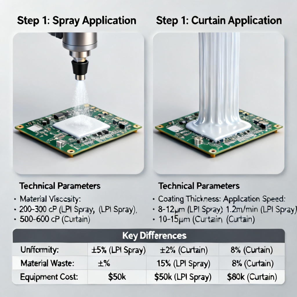
Spray coating solder mask application involves atomizing a liquid solder mask (typically low-viscosity LPI or epoxy-based material) and depositing it onto the PCB surface using compressed air or electrostatic charge. This solder mask application method is particularly effective for boards with irregular shapes, deep cavities, or tall components.
2.2 Spray Coating Solder Mask Application Process
The spray coating solder mask application process begins with mixing the solder mask liquid with a thinner to achieve correct viscosity (typically 100–300 cP). The mixture is filtered to remove particles. The PCB panel is placed on a conveyor belt or rotating fixture; for electrostatic spray, the panel is grounded to attract charged droplets.
A spray gun (manual or robotic) moves across the panel in a predetermined pattern. Key parameters include flow rate of 10–50 ml/min, atomization pressure of 2–4 bar, distance from panel of 15–30 cm, and traverse speed of 10–30 m/min. Multiple passes may be required to achieve desired thickness (typically 20–40 µm), with each pass allowed to flash off solvents before the next.
The wet mask is then tack-dried and exposed to UV light through a phototool, similar to LPI but with potentially shorter exposure time due to thinner and more uniform mask. Development and final cure follow the same process as LPI.
2.3 Key Advantages of Spray Coating Solder Mask Application
Spray coating solder mask application provides excellent coverage of complex topography, penetrating between tall SMD components, around through-hole pins, and into deep recesses. When properly calibrated, spray produces very even coating on flat surfaces and edges, reducing thin spots. Robotic spray systems can coat large panels (e.g., 24” x 30”) quickly. No screen stencils are needed, avoiding cost and lead time. Risk of mask slivers on fine-pitch pads is lower compared to screen printing.
2.4 Limitations of Spray Coating Solder Mask Application
Significant overspray can occur (up to 30–50% material loss) in non-electrostatic systems. Spraying generates volatile organic compounds (VOCs), requiring proper ventilation. Inconsistent spray patterns or thin mask can cause pinholes. Spray tends to produce thinner coating on sharp edges and corners. Cannot achieve same resolution as LPI for sub-100 µm dams.
2.5 When to Use Spray Coating Solder Mask Application
Use spray coating solder mask application for boards with deep cavities, tall components, or complex 3D shapes, prototypes and low-volume runs (100–500 boards), panels with mixed copper thicknesses, and applications requiring uniform thickness over large areas (e.g., RF boards).
3. Curtain Coating Solder Mask Application – High-Speed for Simple Designs
3.1 What is Curtain Coating Solder Mask Application?

Curtain coating solder mask application is a continuous-flow method where a thin, vertical sheet (curtain) of liquid solder mask falls onto a horizontally moving PCB panel. This solder mask application method is highly efficient for high-volume production of simple, flat boards.
3.2 Curtain Coating Solder Mask Application Process
The curtain coating solder mask application process begins with maintaining the solder mask (typically high-viscosity epoxy or acrylic) at precise viscosity (500–2000 cP) and temperature (25–35°C) in a holding tank. The mask is pumped through a narrow slot nozzle (0.5–1.5 mm gap) to create a free-falling curtain. The PCB panel is placed on a conveyor belt moving at constant speed (typically 1–5 m/min) under the curtain. Speed is matched to flow rate to achieve desired wet thickness.
To prevent mask dripping off edges, the panel may have slight upward tilt or be placed on a carrier frame. Some systems use air knives to trim mask at edges. The coated panel is then tack-dried and exposed to UV light through a phototool. Because the mask is thicker than spray, longer exposure times may be needed. Development and final cure follow the same process as LPI.
3.3 Key Advantages of Curtain Coating Solder Mask Application
Curtain coating solder mask application offers high speed and throughput, coating hundreds of panels per hour. The closed-loop curtain system results in minimal waste (typically <5%). Very consistent coating thickness across the entire panel, even on large panels. Lower material cost per board compared to LPI or spray. Once parameters are set, the process is stable and requires minimal operator intervention.
3.4 Limitations of Curtain Coating Solder Mask Application
Curtain coating solder mask application cannot handle boards with tall components, deep cavities, or complex topographies. Typical wet thickness is 50–100 µm, resulting in final dry thickness of 20–40 µm, which can lead to cracking or poor adhesion on fine-pitch pads. Edges may have thicker coating or drips requiring post-coating trimming. Minimum dam width is typically >150 µm (6 mils). Most commonly used with green mask.
3.5 When to Use Curtain Coating Solder Mask Application
Use curtain coating solder mask application for high-volume production of simple double-sided or multilayer boards (e.g., consumer electronics, power supplies), boards with large pads and wide trace spacing (pitch >0.8 mm), applications where cost is primary driver, and panels with uniform copper distribution.
4. Comparative Analysis – Choosing the Right Solder Mask Application Method
| Solder Mask Application Parameter | LPI | Spray Coating | Curtain Coating |
|---|---|---|---|
| Resolution (min. dam) | 75–100 µm | 100–150 µm | >150 µm |
| Thickness Uniformity | Good (screen) to Excellent (vacuum) | Excellent (robotic) | Excellent |
| Topography Handling | Good (flat boards) | Excellent (complex shapes) | Poor (flat only) |
| Throughput | Medium | Medium-High | Very High |
| Material Waste | Low (screen) to Medium (spray) | Medium-High | Very Low |
| Cost per Board | Medium-High | Medium | Low |
| Best For | HDI, fine-pitch, high-reliability | Prototypes, complex shapes, RF | High-volume, simple designs |
5. Advanced Considerations for B2B PCB Buyers
Solder mask application must be compatible with chosen surface finish (HASL, ENIG, OSP, etc.). LPI and spray masks generally work well with all finishes, while curtain-coated masks may require thicker mask to withstand HASL thermal shock. LPI is excellent for tenting vias; spray and curtain may leave thin spots over vias, leading to tent collapse. For critical applications, specify “tented vias” and confirm mask thickness.
Green LPI offers the best UV stability and thermal performance. Black and white masks have higher thermal absorption and may crack under high heat. For high-power boards, consider matte finish to reduce glare during automated optical inspection (AOI). All three solder mask application methods can meet IPC-6012 Class 2 or Class 3, but LPI is the only method that consistently achieves Class 3 requirements for fine-pitch designs. Always request a Certificate of Compliance (CoC) for critical orders.
Curtain coating is the fastest and cheapest for simple boards. Spray is ideal for prototypes. LPI is the most versatile but has longer lead times due to phototool creation. For custom orders, discuss trade-offs with your manufacturer.
6. Frequently Asked Questions About Solder Mask Application
What is the best solder mask application method for HDI boards?
LPI solder mask application is the best method for HDI boards due to its high resolution (75–100 µm dams) and excellent adhesion, essential for fine-pitch components and microvias.
How does spray coating solder mask application handle complex geometries?
Spray coating solder mask application excels with complex geometries, penetrating between tall SMD components, around through-hole pins, and into deep recesses, ensuring no exposed copper.
Is curtain coating solder mask application suitable for prototypes?
Curtain coating solder mask application is not ideal for prototypes due to its requirement for flat boards and high minimum order quantities; spray coating is better suited for low-volume runs.
What factors affect solder mask application cost?
Solder mask application cost depends on method (LPI is highest, curtain lowest), board complexity, volume, material type, and color. LPI costs more due to phototool creation and longer processing time.
Can solder mask application meet IPC Class 3 requirements?
Yes, LPI solder mask application consistently meets IPC-6012 Class 3 requirements for fine-pitch designs, while spray and curtain methods may struggle with resolution and thickness uniformity.
7. Conclusion – Selecting the Optimal Solder Mask Application
The choice between LPI, spray, and curtain solder mask application depends on board design complexity, volume, reliability requirements, and budget. LPI solder mask application remains the gold standard for high-density, high-reliability applications. Spray coating solder mask application offers unparalleled flexibility for complex geometries and low-volume runs. Curtain coating solder mask application delivers unmatched speed and cost efficiency for simple, high-volume designs.
For B2B PCB procurement: use spray coating for prototypes and small batches, LPI via screen printing or electrostatic spray for medium-volume fine-pitch designs, and curtain coating for high-volume simple boards. Contact our engineering team for expert guidance on solder mask application for your next PCB project.