PCB Routing and Profiling VS coring Tab Routing
PCB Routing and Profiling VS coring Tab Routing are the final mechanical steps in printed circuit board fabrication, where individual boards are separated from a larger production panel. This process is critical because it directly impacts board edge quality, component integrity, and assembly yield. Two primary methods dominate the industry: V‑Scoring and Tab Routing (also known as routing with break‑away tabs). Each technique offers distinct advantages depending on board shape, thickness, component proximity, and production volume. Understanding their differences, limitations, and optimal applications is essential for any B2B PCB buyer, designer, or manufacturer.
1. What Is V‑Scoring in PCB Routing and Profiling?
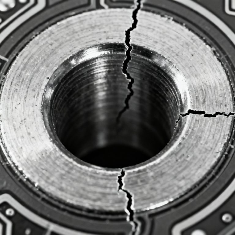
V‑Scoring is a depaneling technique where a V‑shaped groove is cut along both the top and bottom surfaces of the PCB panel along a straight line. This groove reduces the board’s thickness at the score line, typically to about one‑third of the original thickness (e.g., for a 1.6 mm board, the remaining thickness is approximately 0.4 mm). After assembly, boards are snapped apart along these pre‑scored lines, either manually or using a specialized V‑score cutter or breaking machine.
1.1 Key Design Rules and Parameters for V‑Scoring
PCB routing and profiling via V‑Scoring requires precise control of score line depth, angle, and spacing. The depth of the V‑groove is controlled with high precision, typically leaving 0.3–0.5 mm of remaining material. The angle of the V‑cut is usually 30° or 45°, with the exact angle chosen based on board thickness and material. Board shape constraint: V‑Scoring only works for straight, continuous score lines. It cannot accommodate curved, irregular, or complex board outlines. This means the board must have a rectangular or square shape with edges that align perfectly with the panel’s straight edges. Minimum spacing to copper: To avoid damaging copper traces or components, the score line must be kept at least 0.5 mm away from any copper feature (pads, vias, traces) on both sides of the board. Some manufacturers recommend a minimum of 0.75 mm for high‑reliability designs. Panel thickness requirements: V‑Scoring is most suitable for standard PCB thicknesses (0.8 mm to 2.4 mm). Very thin or very thick boards may require special score depths or alternative methods. Number of score lines: The number of parallel score lines is limited by panel size and board dimensions. Typically, a single panel can have multiple score lines, but each line must be straight and continuous across the entire panel.
1.2 Advantages of V‑Scoring in PCB Routing and Profiling
High speed and low cost: V‑Scoring is a fast, automated process that requires minimal setup. It is the most cost‑effective depaneling method for high‑volume production of simple rectangular boards. No tooling waste: Unlike routing, V‑scoring does not produce any material waste between boards because the score line is cut directly into the panel. Clean, smooth edges: When properly broken, the edges are clean and free of fiberglass fraying or burrs. This is particularly important for boards that will be handled or inserted into edge connectors. Space efficiency: V‑scoring allows for very tight board‑to‑board spacing on the panel (often as little as 0.5 mm), maximizing panel utilization and reducing material cost. Compatibility with assembly: After assembly, boards can be snapped apart quickly, either manually or with automated break‑off equipment, without the need for secondary routing.
1.3 Disadvantages and Limitations of V‑Scoring
Straight lines only: The most significant limitation is that V‑scoring cannot handle non‑rectangular board outlines, cutouts, or slots. If your board has a complex shape, V‑scoring alone is insufficient. Edge quality variability: While generally clean, manual snapping can sometimes cause slight chipping or uneven edges, especially if the remaining material thickness is not uniform. Component stress: The snapping action can induce mechanical stress on nearby components, particularly large or heavy parts (e.g., connectors, transformers). This can lead to solder joint fractures or component damage. Limited to one‑sided scoring: V‑scoring typically scores only the top and bottom surfaces. If a board has components on both sides, the scoring line must be carefully positioned to avoid interference. Not suitable for all thicknesses: Boards thinner than 0.8 mm may be too fragile to snap, while boards thicker than 2.4 mm may require excessive force, leading to edge damage.
1.4 Best Practices for V‑Scoring in PCB Routing and Profiling
Always ensure the score line is at least 0.5 mm away from any copper or component. Use a 30° V‑cut for standard FR‑4 boards; 45° cuts are better for thicker boards. For boards with heavy components near the score line, consider using a V‑score cutter with a controlled breaking mechanism rather than manual snapping. Design the panel so that the score line runs parallel to the grain of the fiberglass weave to minimize the risk of delamination. Perform a trial break on a test panel to verify the score depth and edge quality before full production.
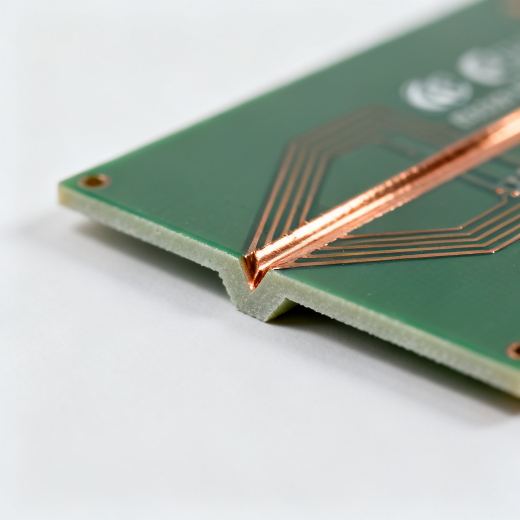
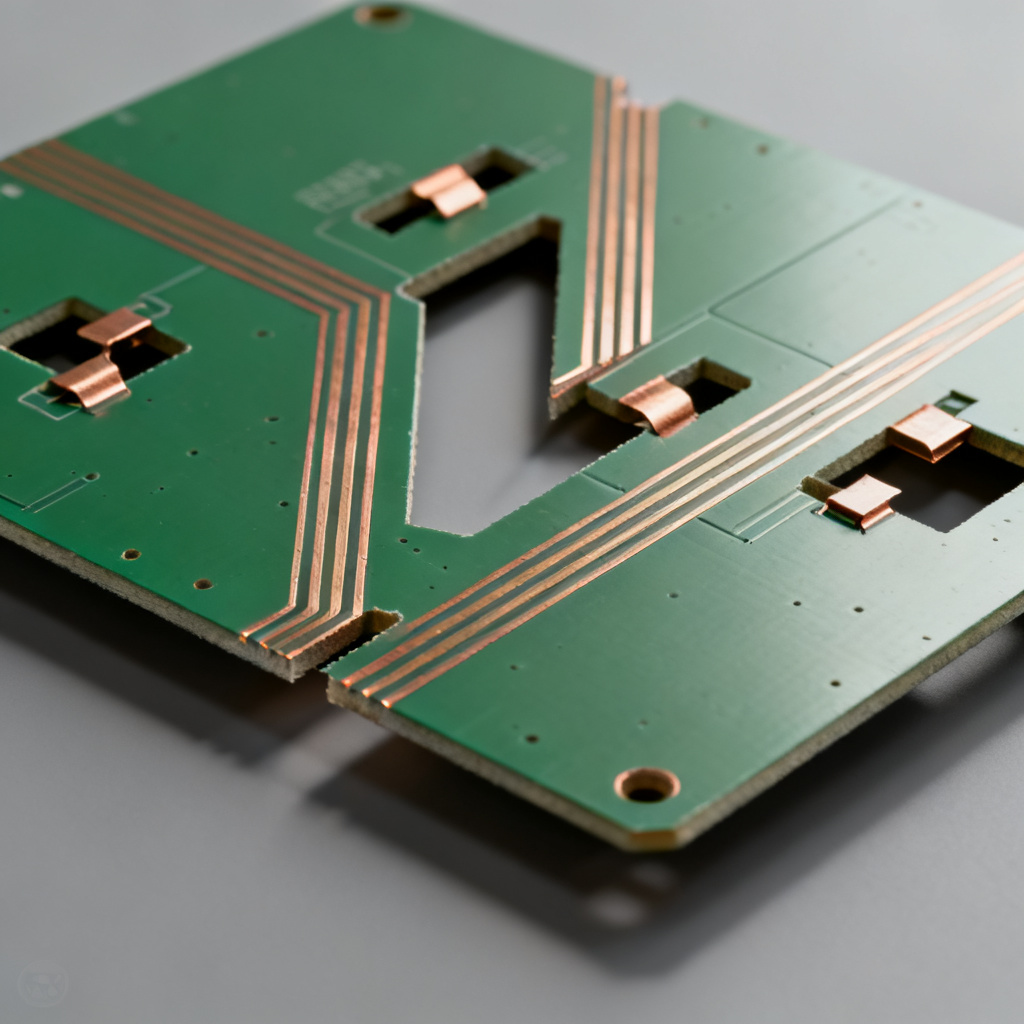
2. What Is Tab Routing in PCB Routing and Profiling?
Tab routing (also called “routing with break‑away tabs” or “mouse‑bite routing”) involves using a CNC router to cut around the individual PCB outline, leaving small connecting tabs (typically 2–5 mm wide) that hold the board to the panel frame or to adjacent boards. After assembly, these tabs are broken off by hand, with pliers, or using a depaneling press. The routed area can be either a complete outline or a partial cut with tabs strategically placed.
2.1 Key Design Rules and Parameters for Tab Routing
Tab width and number: Tabs are typically 2 mm to 5 mm wide, with the number of tabs determined by board size, weight, and component layout. A common rule is to use one tab per 100 mm of board perimeter. For heavy boards, additional tabs may be required. Tab location: Tabs should be placed at the corners and along straight edges, but never near sensitive components, connectors, or edge‑mounted parts. A minimum clearance of 1 mm from copper is recommended. Routing bit diameter: The router bit diameter is usually 1.5 mm to 2.5 mm. Smaller bits allow for tighter curves but are more prone to breakage. The routing path must be continuous and free of sharp internal corners (a minimum radius of 0.5 mm is typical). Board shape flexibility: Tab routing can accommodate any board shape, including circles, polygons, cutouts, and slots. This makes it the preferred method for complex or irregular PCB outlines. Panel border requirements: A panel border of at least 5 mm is required around the entire array to provide sufficient material for tooling holes and routing clearance. This border is often called the “tooling strip” or “frame.”
2.2 Advantages of Tab Routing in PCB Routing and Profiling
Unlimited shape capability: Tab routing can produce any board outline, including internal cutouts, slots, and non‑rectangular shapes. This is the only viable method for boards with complex geometries. Low stress on components: The routing process itself exerts no mechanical stress on the board or components. The breaking of tabs is a localized, low‑force action that can be performed away from sensitive areas. High edge quality: The routed edges are smooth, precise, and free of fiberglass fraying. They are typically superior to V‑scored edges in terms of dimensional accuracy. Compatibility with mixed shapes: A single panel can contain boards of different shapes and sizes, as long as they fit within the panel dimensions. This is not possible with V‑scoring. Allows for edge plating: Tab routing is compatible with edge‑plated connectors (e.g., gold fingers) because the routing path can be precisely controlled.
2.3 Disadvantages and Limitations of Tab Routing
Higher cost: Tab routing is slower than V‑scoring because each board outline must be routed individually. The CNC routing time adds to the fabrication cost, especially for large panels or complex shapes. Material waste: The routing process removes material (the “routout” or “webbing”) between boards, resulting in some material waste. This can reduce panel utilization by 5–15% compared to V‑scoring. Tab breakage issues: If tabs are too thin or improperly placed, they can break prematurely during handling or assembly. Conversely, tabs that are too thick may be difficult to break cleanly, leaving rough edges. Tool wear: Router bits wear over time and must be replaced periodically. Worn bits can produce rough edges or cause delamination. Dust and debris: The routing process generates fiberglass dust and debris, which must be cleaned from the board surface to avoid contamination of solder joints or components.
2.4 Best Practices for Tab Routing in PCB Routing and Profiling
Place tabs at a minimum of 2 mm width, and increase to 3–5 mm for boards over 100 grams. Use a minimum of four tabs per board, one at each corner, for square/rectangular boards. For irregular shapes, add tabs at stress concentration points. Ensure a routing clearance of at least 0.5 mm from any copper feature. For high‑voltage boards, increase this to 1 mm. Use a 2 mm diameter router bit for standard FR‑4, and a 1.5 mm bit for tight internal radii. After routing, perform a visual inspection of all tabs to ensure they are intact and free of cracks. For boards with heavy components, consider using a depaneling press with a dedicated tab‑breaking fixture to avoid manual stress.
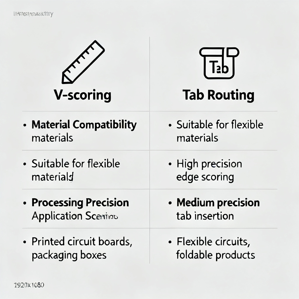
3. Comparing V‑Scoring vs. Tab Routing – A Detailed Matrix for PCB Routing and Profiling
| Feature | V‑Scoring | Tab Routing |
|---|---|---|
| Board Shape | Rectangular/straight edges only | Any shape (circle, polygon, cutouts) |
| Edge Quality | Good (clean, but may chip) | Excellent (smooth, precise) |
| Production Speed | Very fast (seconds per panel) | Slower (minutes per panel) |
| Cost per Board | Low (high‑volume) | Moderate to high |
| Panel Utilization | High (tight spacing) | Lower (due to routout waste) |
| Component Stress | Moderate (snapping force) | Low (localized tab break) |
| Tooling Cost | Low (no router bits) | Higher (bits and CNC time) |
| Flexibility | Low (straight lines only) | High (any geometry) |
| Ideal for | High‑volume, simple boards | Complex, low‑to‑mid volume |
| Edge Plating | Not recommended | Yes, compatible |
| Thickness Range | 0.8–2.4 mm | 0.4–3.2 mm (or more) |
| Minimum Board Size | No strict limit | Limited by router bit size |
4. When to Choose Which Method – Practical Decision Guidance for PCB Routing and Profiling
4.1 Choose V‑Scoring When:
Your board has a simple rectangular or square shape with no cutouts. You are producing high volumes (thousands of boards per month) and need to minimize cost. The board edges do not require edge plating or gold fingers. Components are located at least 2 mm away from the score line. You want to maximize panel utilization and reduce material waste.
4.2 Choose Tab Routing When:
Your board has a non‑rectangular outline (e.g., circular, L‑shaped, with slots). The board contains edge‑mounted connectors, gold fingers, or plated edges. You have components near the board edge that cannot tolerate snapping stress. The board is very thin (<0.8 mm) or very thick (>2.4 mm). You need to panelize boards of different shapes on the same panel.
4.3 Hybrid Approach: V‑Scoring + Tab Routing
Some advanced PCB fabricators offer a hybrid method where V‑scoring is used for straight panel separation lines, and tab routing is used for complex internal board outlines. This approach combines the speed and cost benefits of V‑scoring with the shape flexibility of tab routing. For example, a panel may contain rectangular boards that are V‑scored for easy snapping, but each board may have a cutout that is routed with tabs. This hybrid method is particularly useful for medium‑complexity designs.
5. Advanced Considerations and Quality Control in PCB Routing and Profiling
5.1 Edge Quality Standards
Both V‑scoring and tab routing must meet IPC‑6012 edge quality standards. Acceptable edge conditions include: No visible delamination or fiberglass fraying. No copper lifting or burrs exceeding 0.1 mm. For V‑scored boards, the score line must be centered and uniform across the panel. For routed boards, the edge must be free of router bit marks deeper than 0.05 mm.
5.2 Depaneling Equipment
Manual Snapping: Suitable for low‑volume V‑scored boards. Use a clean, flat surface and apply even pressure. V‑Score Cutter (Guillotine): A semi‑automated tool that provides a controlled break, reducing stress on components. Depaneling Press: Ideal for tab‑routed boards. The press applies uniform force to all tabs simultaneously, minimizing board flex. CNC Router: For high‑volume tab routing, a dedicated CNC depaneling router can be programmed to cut multiple panels automatically.
5.3 Inspection and Testing
After depaneling, each board should be inspected for: Cracks or delamination at the break points. Integrity of solder joints near the board edge. Dimensional accuracy of the final outline. Cleanliness (no dust or debris on the board surface). For high‑reliability applications (e.g., medical, aerospace), consider performing a micro‑section analysis of the edge to verify that the copper layers are not damaged.
6. Cost and Lead Time Implications for PCB Routing and Profiling
V‑Scoring: Typically adds $0.01–$0.05 per board in fabrication cost, depending on panel size and volume. Lead time is minimal because no routing program is needed. Tab Routing: Adds $0.05–$0.20 per board, plus a one‑time setup fee for the CNC program. Lead time may increase by 1–2 days for complex shapes. Hybrid: Cost falls between the two, but the added complexity may increase lead time. For B2B buyers, it is often more economical to choose V‑scoring for simple boards and reserve tab routing for designs that truly require it. However, if your board has any irregular features, tab routing is the only reliable option.
7. FAQ – PCB Routing and Profiling: V‑Scoring vs. Tab Routing
What is the main difference between V‑Scoring and Tab Routing in PCB routing and profiling?
Which method is more cost‑effective for high‑volume PCB routing and profiling?
Can Tab Routing be used for boards with edge‑plated connectors?
What is a hybrid approach in PCB routing and profiling?
What edge quality standards apply to PCB routing and profiling?
8. Conclusion: Making the Right Choice for Your PCB Routing and Profiling Project
Both V‑scoring and tab routing are essential techniques in PCB depaneling, each with clear strengths and trade‑offs. V‑scoring excels in high‑volume, low‑cost production of simple rectangular boards, while tab routing offers the flexibility needed for complex, high‑reliability designs. By understanding the design rules, limitations, and best practices outlined in this pillar page, you can confidently select the method that aligns with your product requirements, budget, and timeline. For any custom PCB project, we recommend consulting with your fabrication partner early in the design phase to optimize the panel layout and depaneling method. A well‑planned routing and profiling strategy not only reduces cost but also ensures the long‑term reliability of your electronic assemblies.
Need expert guidance on PCB routing and profiling? Contact our engineering team today for a free design review and panelization optimization. We specialize in high‑quality V‑scoring and tab routing for B2B customers worldwide.