Master the critical relationship between PCB power plane resonance and decoupling network design. Learn how to mitigate impedance peaks, optimize capacitor selection, and ensure stable power delivery for high-speed digital and RF circuits. This comprehensive guide synthesizes expert knowledge for reliable PCB performance.
1. Understanding PCB Power Plane Resonance
1.1 Physics of Plane Resonance
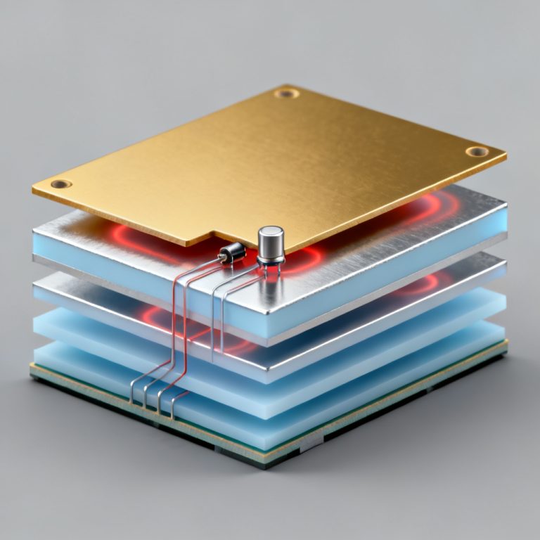
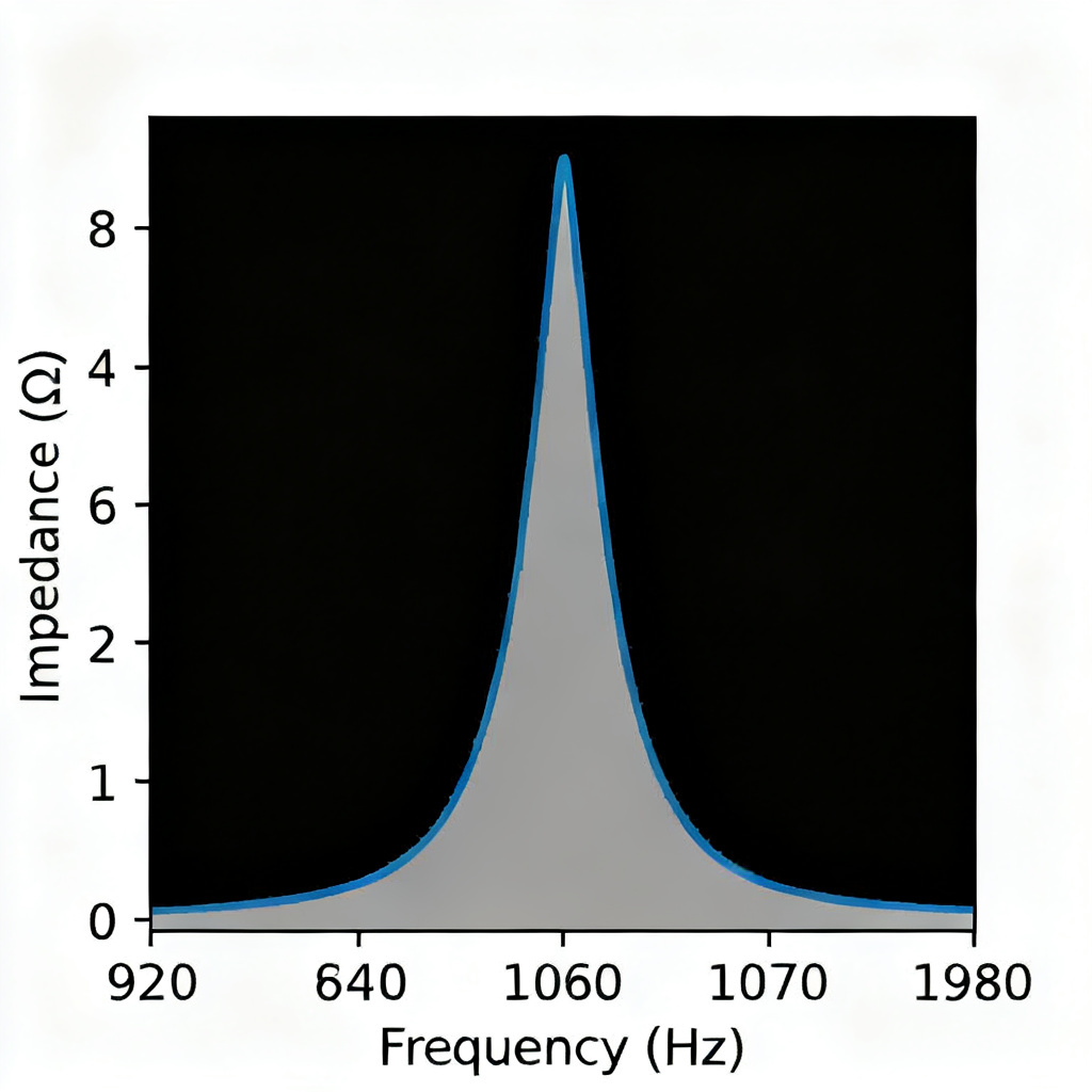
PCB power plane resonance occurs when a power plane pair (VCC and GND) acts as a parallel-plate waveguide. Standing waves form at specific frequencies determined by board dimensions and dielectric permittivity. At these resonant frequencies, impedance spikes dramatically—from milliohms to tens of ohms—creating the primary source of PDN noise.
1.2 The Impedance Profile Target
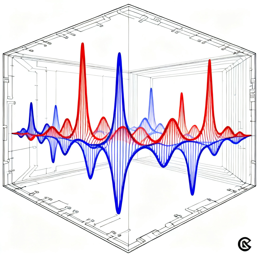
The goal of PDN design is to maintain a target impedance (Z_target) across the entire frequency range. Z_target = Allowable Ripple Voltage / Transient Current. For example, a 1.8V rail with 5% ripple (90mV) and a 10A transient current requires Z_target of 9 milliohms or less.
1.3 Where Resonance Occurs
- Low Frequencies (DC to ~1 MHz): Dominated by VRM and bulk capacitors.
- Mid Frequencies (1 MHz to ~100 MHz): Dominated by decoupling capacitors (MLCCs) and mounting inductance.
- High Frequencies (>100 MHz): Dominated by power plane intrinsic capacitance and resonant behavior.
1.4 The Anti-Resonance Problem
When a decoupling capacitor is placed on a resonant plane, the combination of the capacitor’s ESL and the plane’s capacitance can create a parallel anti-resonance peak. This is the most common failure point in decoupling networks.
2. Decoupling Network Design for PCB Power Plane
2.1 The Role of Decoupling Capacitors
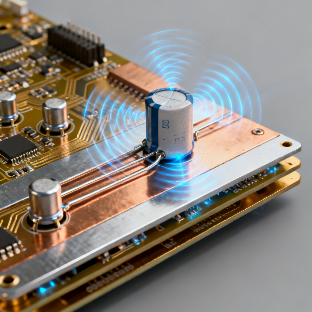
Decoupling capacitors serve two primary functions: providing local charge reservoir during current transients and shunting high-frequency noise to ground plane. PCB power plane resonance suppression relies heavily on proper capacitor selection and placement.
2.2 Capacitor Types and Frequency Response
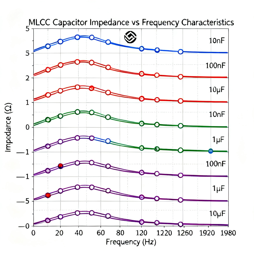
Every real capacitor has three parasitic elements: ESR (damping), ESL (inductance), and SRF (self-resonant frequency). Common MLCC sizes and typical SRF (with ~1nH mounting inductance): 0402 0.1µF ~50 MHz, 0603 1µF ~16 MHz, 0805 10µF ~5 MHz, 1206 100µF ~1.5 MHz.
2.3 The Multi-Value Trap
A common mistake is using a wide range of capacitor values, which often creates anti-resonance peaks. The better approach is using multiple identical capacitors of a single, mid-range value in parallel. This reduces total ESL and ESR without creating anti-resonance.
3. Advanced Techniques for PCB Power Plane Resonance Suppression
3.1 Via Inductance Minimization
The biggest contributor to mounting inductance is the via loop. Best practices: use multiple vias per capacitor pad, place vias as close as possible to pads, use short and wide traces, and consider buried vias or microvias for high-speed designs.
3.2 Embedded Capacitance
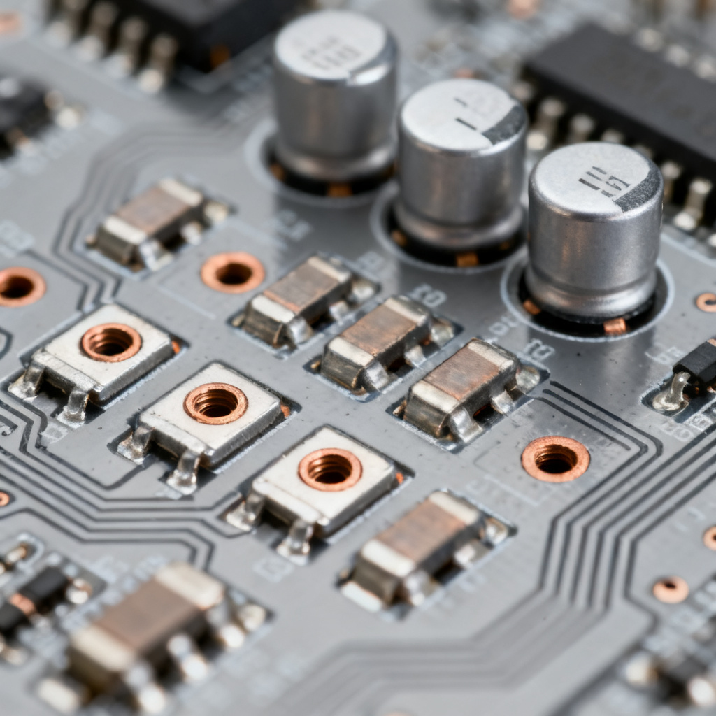
For frequencies above 200 MHz, discrete capacitors become ineffective. Embedded capacitance uses a thin dielectric layer between power planes, providing near-zero ESL and broadband decoupling from ~100 MHz to several GHz. This is the ultimate solution for PCB power plane resonance at high frequencies.
3.3 Plane Segmentation and Stitching
If power plane slots are unavoidable, use stitching capacitors (typically 0.1µF or 1µF) across the slot every 1/20th of the wavelength of the highest frequency of concern.
4. Practical Design Methodology
4.1 Step 1: Define Target Impedance
Calculate Z_target from your IC’s voltage and current requirements. This is your design constraint for PCB power plane resonance management.
4.2 Step 2: Model VRM and Bulk Capacitance
The VRM has finite output impedance (typically 1-10 milliohms at low frequencies). Add bulk capacitors (10-100µF) to supply current during long-duration transients.
4.3 Step 3: Select Mid-Frequency Decoupling
Choose a single MLCC value (e.g., 0.1µF or 1µF in 0402 or 0603 size). Calculate number of caps needed using N = ESR_cap / Z_target.
4.4 Step 4: Place Capacitors Strategically
Place decaps as close as possible to power pins of active devices. For BGA packages, place decaps on bottom side directly under power pins using microvias. Distribute decaps evenly across the power plane area.
4.5 Step 5: Simulate or Measure Impedance Profile
Use 2D/3D field solvers (e.g., Ansys SIwave, Cadence Sigrity) to simulate PDN impedance from DC to 1 GHz. Look for impedance peaks above Z_target and anti-resonance between capacitor groups.
4.6 Step 6: Mitigate High-Frequency Resonance
If simulation shows impedance peaks above 200 MHz, consider reducing plane spacing, adding embedded capacitance layers, using multiple vias per capacitor, or adding ferrite beads with caution.
5. Common Pitfalls in PCB Power Plane Resonance Design
| Pitfall | Consequence | Solution |
|---|---|---|
| Using too many different capacitor values | Anti-resonance peaks | Use fewer values (ideally one mid-value) in parallel |
| Ignoring via inductance | SRF shifts lower, reducing high-frequency performance | Use multiple vias per pad; minimize via length |
| Placing capacitors far from load | Increased loop inductance; ineffective decoupling | Place within 1-2 mm of power pins |
| Overlooking plane resonance | High impedance at specific frequencies | Simulate PDN; use embedded capacitance if needed |
| Using high-ESR capacitors for bulk decoupling | Ineffective at low frequencies; poor ripple rejection | Use low-ESR tantalum or aluminum polymer caps |
| Not considering temperature and DC bias | MLCC capacitance drops significantly under DC bias | Use higher voltage-rated capacitors (e.g., 2x rail voltage) |
6. Real-World Example: Decoupling a 1.8V FPGA Rail
Constraints: Rail 1.8V, 5A max transient, allowable ripple 3% (54mV), target impedance 10.8 milliohms (54mV / 5A), frequency range DC to 500 MHz.
Design: Standard buck converter with 10µH output inductor and 100µF ceramic output cap. Two 100µF tantalum polymer caps (ESR ~50mΩ each, parallel gives 25mΩ). Ten 0.1µF 0402 X7R 6.3V MLCCs (each ~20mΩ ESR at SRF ~50 MHz, ten in parallel give ~2mΩ at SRF). High-frequency handled by plane intrinsic capacitance (1″ x 1″ area with 4-mil dielectric gives ~1nF). All caps placed on bottom side under BGA VCC pins, each with two vias to plane.
Simulation Result: Impedance stays below 10mΩ from DC to 1 GHz. No resonance peaks above target.
7. Conclusion: The Path to a Stable PDN
PCB power plane resonance and decoupling network design are inseparable. Key takeaways: plane resonance creates impedance peaks that discrete caps alone cannot fix; decoupling network design is about minimizing inductance; simulation is essential for frequencies above 100 MHz; embedded capacitance is most effective for high-frequency suppression; practical implementation determines success.
8. FAQ: PCB Power Plane Resonance and Decoupling
What is PCB power plane resonance?
PCB power plane resonance occurs when power and ground planes form a resonant cavity, causing impedance spikes at specific frequencies that can disrupt power delivery.
How does decoupling network design suppress PCB power plane resonance?
Proper decoupling network design uses capacitors with low ESL and ESR, strategic placement, and multiple identical values to provide low-impedance paths that dampen resonant peaks.
What are the best capacitor values for PCB power plane resonance mitigation?
Using a single mid-range value (e.g., 0.1µF or 1µF) in parallel is more effective than multiple different values, as it avoids anti-resonance peaks.
Why is via inductance critical in PCB power plane resonance design?
Via inductance can double or triple effective capacitor inductance, shifting SRF lower and reducing high-frequency decoupling effectiveness. Multiple vias per pad minimize this issue.
When should embedded capacitance be used for PCB power plane resonance?
Embedded capacitance is recommended for frequencies above 200 MHz, where discrete capacitors become ineffective due to ESL limitations.
9. Comparison: Standard vs. Advanced Decoupling Approaches
| Parameter | Standard Decoupling | Advanced Decoupling (Our Approach) |
|---|---|---|
| Capacitor values | Multiple different values | Single mid-range value in parallel |
| Via management | Single via per pad | Multiple vias per pad, minimized loop area |
| High-frequency handling | Limited to ~100 MHz | Up to several GHz with embedded capacitance |
| Simulation | Rarely performed | Mandatory 2D/3D field solver simulation |
| Risk of anti-resonance | High | Low |
10. Glossary of Key Terms
- ESL (Equivalent Series Inductance): Parasitic inductance in capacitors that limits high-frequency performance.
- ESR (Equivalent Series Resistance): Parasitic resistance that provides damping in decoupling networks.
- SRF (Self-Resonant Frequency): Frequency at which capacitor impedance is minimum (equal to ESR).
- Anti-Resonance: High-impedance peak created when inductive and capacitive impedances cancel in parallel.
- Embedded Capacitance: Thin dielectric layer between power planes providing ultra-low-inductance decoupling.
- PDN (Power Distribution Network): Complete system delivering power from VRM to ICs.