PCB Thermal Management Guide Vias Heatsinks Spreaders
PCB Thermal Management Guide: Vias, Heatsinks & Spreaders
Effective PCB thermal management is critical for high-power electronics reliability. This comprehensive guide covers thermal vias, heatsinks, and spreaders—the core strategies for dissipating heat in modern PCB designs. Whether you are designing for power converters, LED lighting, or automotive electronics, these principles ensure optimal performance and longevity.
In the world of high-power electronics, thermal management is no longer an afterthought—it is a fundamental design requirement. As components shrink and power densities increase, effective heat dissipation directly impacts reliability, performance, and lifespan. A poorly managed thermal profile can lead to solder joint fatigue, component failure, and catastrophic board delamination.
This guide covers the three primary thermal management strategies: thermal vias, heatsinks, and heat spreaders. We will explore how each works, when to use them, and how to optimize them for your specific PCB application. Whether you are designing for LED lighting, power converters, or automotive electronics, these principles apply universally.
1. Thermal Vias Foundation for PCB Thermal Management
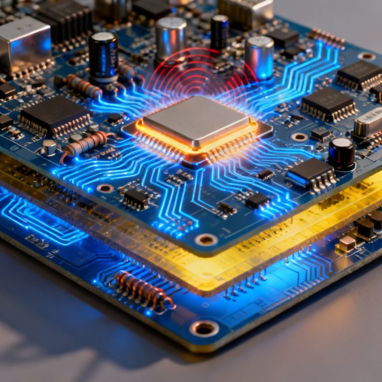
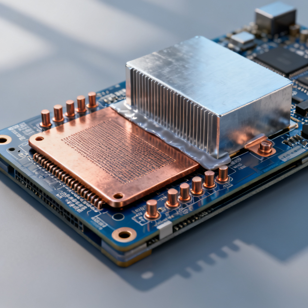
Thermal vias are the foundation of effective PCB thermal management. These plated through-holes (PTH) or microvias conduct heat away from hot components to cooler areas of the PCB, such as internal copper planes or a bottom-side heatsink. Unlike standard signal vias, thermal vias are intentionally placed under or near heat-generating components (e.g., power ICs, MOSFETs, LEDs) to create a low-thermal-resistance path.
1.1 How Thermal Vias Work in PCB Thermal Management
Thermal conductivity dynamics: Heat travels through copper much more efficiently than through FR4 or other PCB substrates.
The vertical bridge: A thermal via acts as a direct pathway, allowing heat to move vertically through the board.
Key Physics: Copper thermal conductivity: ~400 W/m·K. FR4 thermal conductivity: ~0.3 W/m·K. A 0.3mm diameter via with 1oz copper plating can reduce thermal resistance by 50-80% compared to an unplated hole.
1.2 Thermal Via Design Parameters for Optimal Heat Transfer
To maximize heat transfer in your PCB thermal management strategy, consider these variables:
| Parameter | Description | Recommendation for Thermal Management |
|---|---|---|
| Via Diameter | Larger diameters allow more copper mass and lower resistance. | 0.3mm to 0.5mm for general use; multiple smaller vias for high-density designs. |
| Number of Vias | Total cross-sectional copper area determines heat flow. | Use an array (e.g., 4×4 or 6×6 grid) under the component pad. |
| Plating Thickness | Thicker plating increases both thermal and electrical conductivity. | Standard 1oz (35µm); specify 2oz or thicker for extreme power. |
| Via Fill and Capping | Filled vias prevent solder wicking; conductive fills enhance heat transfer. | Use filled and capped vias for surface-mount components requiring flat surfaces. |
| Via Pitch and Pattern | Spacing and arrangement affect efficiency. | Space 0.5mm to 1.0mm apart; staggered patterns often outperform straight grids. |
1.3 Thermal Via Placement Strategies for PCB Thermal Management
Directly under the component pad is the most effective location. Use a thermal pad that matches the component’s exposed pad. Around the component perimeter, place vias near the leads or thermal tabs for components without exposed pads. Connecting to internal planes ensures vias connect to the ground or power plane layers. A single via connecting to a single layer is less effective than a via connecting to multiple copper layers.
1.4 Thermal Via Modeling and Simulation
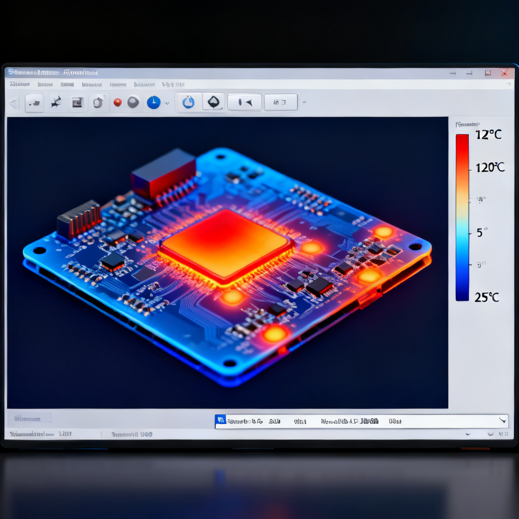
Before fabrication, use thermal simulation tools (e.g., ANSYS Icepak, Flotherm, or free tools like PCB thermal calculators) to estimate junction temperatures. Input via count, diameter, copper weight, and board layer stack-up to predict thermal resistance.
Example Calculation: For a 10W component on a 4-layer board with 16 thermal vias (0.3mm diameter, 1oz plating), the thermal resistance from component to bottom copper plane is approximately 5-8°C/W, depending on board thickness.
1.5 Manufacturing Considerations for Thermal Vias
Drill tolerance: Specify +/-0.05mm for via diameter. Aspect ratio: For standard drilling, keep via depth : diameter ratio under 10:1. For microvias, laser drilling allows higher ratios. Copper plating uniformity: Ensure consistent plating thickness, especially in high-aspect-ratio vias. Solder mask: Leave vias uncovered (exposed copper) for maximum heat transfer, or use solder mask if electrical isolation is needed.
1.6 Common Mistakes with Thermal Vias in PCB Thermal Management
Too few vias: Underestimating the required number leads to hot spots. Poor plane connection: Vias that only connect to a small copper island instead of a full plane. Ignoring via resistance: Each via adds a small resistance; sum them for total thermal path. Not accounting for solder wicking: Unfilled vias can cause solder to flow away from the component joint, reducing reliability.
2. Heatsinks for External PCB Thermal Management
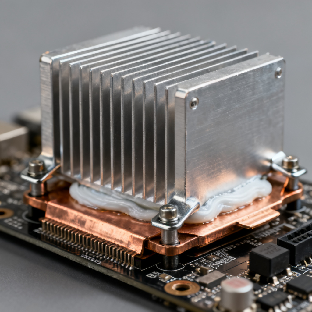
Heatsinks are essential for external PCB thermal management. These passive heat exchangers transfer heat from a component to the surrounding air (or liquid) via convection and radiation. They are typically made of aluminum or copper and are attached to the top or bottom of a PCB-mounted component.
2.1 Types of Heatsinks for PCB Thermal Management
Extruded aluminum heatsinks are most common. Aluminum fins are extruded in a single piece. Cost-effective for medium power (5-50W). Available in various fin shapes (straight, pin, flared). Stamped heatsinks are made from sheet metal (aluminum or copper) stamped into shape. Thin fins, low cost, but lower performance. Suitable for low-power applications. Bonded fin heatsinks have individual fins bonded to a base plate. Allows high fin density and custom shapes. Used in high-performance applications. Skived heatsinks are machined from a solid block of copper or aluminum. Very high fin density and thermal performance. Expensive, used for high-power (>100W) or space-constrained designs. Liquid-cooled heatsinks use water or coolant flowing through channels. Highest performance but complex and expensive. Reserved for extreme power densities (>500W). Passive vs. active heatsinks: Passive rely on natural convection. No moving parts, silent, reliable. Active include a fan or blower. Higher heat dissipation but adds noise, power consumption, and failure risk.
2.2 Heatsink Attachment Methods
Thermal Interface Materials (TIMs) include thermal paste (grease), low cost, good performance (2-4 W/m·K), requires careful application. Thermal pads are pre-cut, easy to use, but lower conductivity (1-3 W/m·K). Phase-change materials are solid at room temperature, liquid at operating temperature, good for high-pressure applications. Thermal epoxy is permanent bonding, high conductivity (3-5 W/m·K). Graphite or metal shims are for high-power applications, direct metal-to-metal contact with minimal TIM. Mechanical attachment includes clips or springs, apply consistent pressure, allow rework. Screws and standoffs are common for larger heatsinks, use spring washers to maintain pressure. Adhesive tape is only for low-power, temporary applications. Soldering for high-reliability applications provides the lowest thermal resistance but is difficult to rework.
2.3 Heatsink Sizing and Selection for PCB Thermal Management
Step 1: Calculate Required Thermal Resistance. Determine component junction temperature limit (Tj_max). Measure ambient temperature (Ta). Calculate required heatsink-to-ambient thermal resistance: R_th(hs-a) = (Tj_max – Ta) / P – R_th(j-c) – R_th(c-hs). Where P is power dissipated, R_th(j-c) is junction-to-case resistance, and R_th(c-hs) is case-to-heatsink resistance (from TIM). Step 2: Choose Heatsink Geometry. Fin height, spacing, and number affect surface area. For natural convection, fin spacing should be >5mm to avoid boundary layer interference. For forced convection, tighter spacing (2-3mm) works better. Step 3: Account for Orientation. Vertical fins (with air flow upward) provide the best natural convection. Horizontal fins reduce performance by 20-40%. In enclosures, consider airflow path and proximity to other components. Step 4: Material Choice. Aluminum (6063-T5) is cost-effective, lightweight, good conductivity (~200 W/m·K). Copper (C11000) has higher conductivity (~400 W/m·K) but is heavier and more expensive. Often used in hybrid heatsinks (copper base, aluminum fins).
2.4 Heatsink Optimization Tips
Use a heat spreader first: A copper spreader under the component can reduce hot spots before the heatsink. Increase surface area: Add fins, pins, or corrugations. Improve airflow: Use a fan or design for natural draft. Consider mounting orientation: Vertical fins in a horizontal enclosure can trap heat. Use multiple smaller heatsinks instead of one large one when space is constrained.
2.5 Common Heatsink Mistakes
Insufficient TIM: Too little or too much paste increases thermal resistance. Incorrect mounting pressure: Too low increases contact resistance; too high can crack the component. Ignoring radiation: In natural convection, radiation can account for 20-30% of heat transfer. Use black anodized surfaces to enhance emissivity. Blocking airflow: Placing heatsinks too close to walls or other components reduces effectiveness.
3. Heat Spreaders for Lateral PCB Thermal Management
Heat spreaders are critical for lateral PCB thermal management. These conductive layers or structures distribute heat laterally across a PCB, reducing temperature gradients and allowing heat to reach thermal vias, heatsinks, or the board edge. They are typically made of copper or aluminum and are integrated into the PCB stack-up or attached as separate components.
3.1 Types of Heat Spreaders
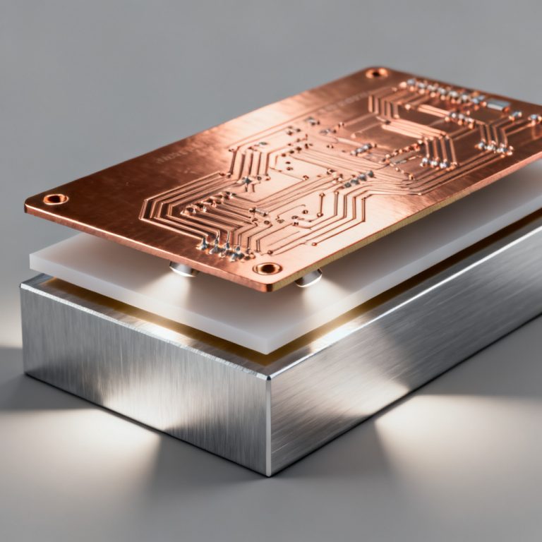
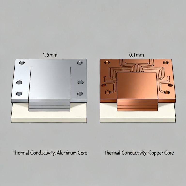
Copper coin (coin insert) is a solid copper cylinder or block inserted into a cavity in the PCB. Provides a direct, low-resistance path from a hot component to an external heatsink or the bottom copper plane. Excellent for high-power components like IGBTs or power modules. Advantages: Very low thermal resistance (0.5-2°C/W), high current capacity. Disadvantages: Requires precise machining, adds cost, may cause CTE mismatch. Copper inlay is a copper sheet or foil laminated into the PCB stack-up, often in the inner layers. Acts as a large-area heat spreader. Common in metal-core PCBs (MCPCBs) and thick copper designs. Advantages: Uniform heat distribution, no extra assembly. Disadvantages: Limits routing flexibility, increases board thickness. Metal-core PCB (MCPCB) has an aluminum or copper base layer replacing the standard FR4 core. The dielectric layer (typically 25-100µm) provides electrical isolation while allowing heat to spread into the metal base. Advantages: Excellent lateral heat spreading, ideal for high-power LEDs. Disadvantages: Higher cost, limited to single-sided component mounting, lower CTE matching. Graphite or diamond spreaders are thin sheets of pyrolytic graphite or synthetic diamond. Extremely high in-plane thermal conductivity (500-2000 W/m·K) but low through-plane conductivity. Used in mobile devices or space-constrained applications. Embedded copper planes are thick copper layers (2oz, 3oz, or more) in the PCB stack-up. These act as both power distribution and heat spreaders. The larger the copper area, the better the heat spreading.
3.2 Design Rules for Heat Spreaders in PCB Thermal Management
Connect spreaders to thermal vias: A spreader without vias is useless for vertical heat transfer. Use multiple spreader layers: A top and bottom copper plane connected by vias creates a “thermal sandwich.” Minimize thermal resistance between spreader and component: Use a filled via-in-pad or copper coin directly under the component. Keep spreader area large: The spreader should extend at least 5-10mm beyond the component footprint for effective lateral spreading. Avoid gaps: Any break in the copper (e.g., for signal routing) creates a thermal bottleneck. Use thermal relief patterns only when necessary.
3.3 Heat Spreader Material Comparison for PCB Thermal Management
| Material | Thermal Conductivity (W/m·K) | Cost | Weight | Typical Use |
|---|---|---|---|---|
| Copper (C11000) | 390-400 | Medium | Heavy | General-purpose spreading |
| Aluminum (6061) | 150-200 | Low | Light | MCPCBs, cost-sensitive designs |
| Graphite (Pyrolytic) | 500-1500 | High | Light | Thin devices, mobile |
| Diamond (CVD) | 2000+ | Very high | Light | Extreme power, laser diodes |
| Silver | 429 | Very high | Heavy | Specialized, rare |
3.4 Integrating Spreaders with Vias and Heatsinks
The most effective PCB thermal management systems combine all three elements: Component → Spreader: A copper coin or thick pad under the component. Spreader → Vias: An array of thermal vias connects the spreader to internal copper planes. Vias → Bottom Plane: The bottom copper layer acts as a secondary spreader. Bottom Plane → Heatsink: A TIM and external heatsink attached to the bottom of the board.
Example Stack-Up: Top layer: 2oz copper, large thermal pad under component. Inner layers: 2oz copper planes connected by thermal vias. Bottom layer: 2oz copper with a solderable pad for heatsink attachment. Vias: 0.3mm diameter, 1oz plating, 4×4 array under component.
3.5 Thermal Simulation for Spreaders
Use finite element analysis (FEA) tools to optimize spreader geometry. Key parameters: Spreader thickness (0.5mm to 2mm), spreader width and length (relative to component size), number and location of vias, board layer stack-up and copper weight. Simulation Output: Temperature distribution across the board, maximum junction temperature, thermal resistance from junction to ambient.
4. Practical Application: Combining All Three Techniques for PCB Thermal Management
4.1 Step-by-Step Design Flow for PCB Thermal Management
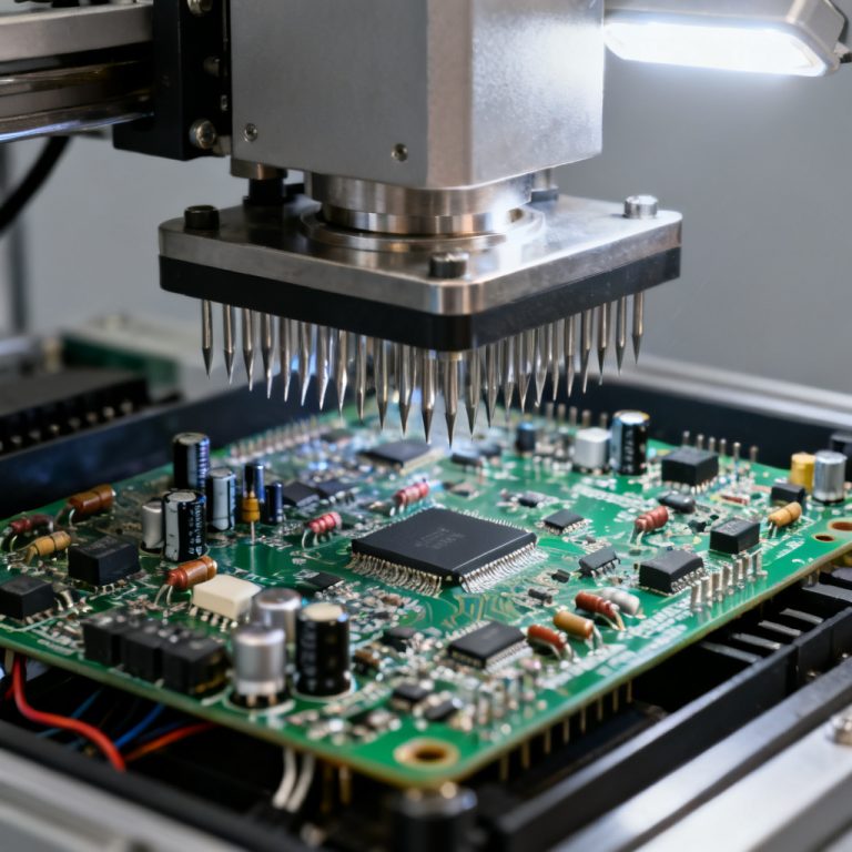
1. Determine power dissipation of the hottest component. 2. Calculate maximum allowable junction temperature (from datasheet). 3. Select thermal management strategy: Low power (<1W): No special measures needed. Medium power (1-5W): Use thermal vias and a small copper spreader. High power (5-20W): Add a heatsink and thick copper planes. Very high power (>20W): Use copper coins, MCPCB, or liquid cooling. 4. Design the thermal via array (number, diameter, pitch). 5. Integrate heat spreaders (copper planes, coins, or inlays). 6. Select and attach heatsink (TIM, mechanical mounting). 7. Simulate and verify thermal performance. 8. Prototype and test with thermocouples or thermal camera.
4.2 Case Study: 10W Power LED PCB Thermal Management
Component: 10W LED with exposed pad. Thermal vias: 16 vias (0.3mm diameter, 1oz plating) in a 4×4 grid under the pad. Heat spreader: 2oz copper on top and bottom layers, connected by vias. Heatsink: Extruded aluminum, 40x40mm, 20mm fin height, with thermal pad (3 W/m·K). Result: Junction temperature = 85°C at 25°C ambient (60°C rise). Within LED’s 100°C limit.
4.3 Common Pitfalls to Avoid
Relying on only one technique: Vias without spreaders, or spreaders without vias, are inefficient. Ignoring board thickness: Thicker boards require more vias or larger copper areas. Not accounting for ambient conditions: High ambient temperature reduces heatsink effectiveness. Forgetting about CTE mismatch: Copper and FR4 expand at different rates; use stress-relief patterns.
5. Advanced Topics in PCB Thermal Management
5.1 Thermal Management for High-Frequency PCBs
At RF frequencies, ground planes must remain continuous. Use thermal vias with careful spacing to avoid creating resonant cavities. Copper coins can be used but must be isolated from RF paths.
5.2 Thermal Management for Flex and Rigid-Flex PCBs
Flexible substrates (polyimide) have lower thermal conductivity than FR4. Use stiffeners (aluminum or copper) in high-heat areas. Thermal vias are possible but limited by flex layer thickness.
5.3 Thermal Management in Harsh Environments
High humidity: Use conformal coating to protect vias and copper from corrosion. Vibration: Solder heatsinks directly or use locking hardware. Thermal cycling: Choose TIMs with low modulus to accommodate expansion.
5.4 Emerging Technologies in PCB Thermal Management
Embedded heat pipes: Thin, sealed tubes that transfer heat via phase change. Thermal interface materials with graphene: Higher conductivity than traditional pastes. 3D-printed heatsinks: Custom shapes for complex enclosures.
Conclusion: Choosing the Right PCB Thermal Management Strategy
Effective PCB thermal management is a system-level challenge. Thermal vias provide the vertical path, heat spreaders distribute heat laterally, and heatsinks reject heat to the environment. The best designs integrate all three, with careful attention to material selection, geometry, and manufacturing constraints. For B2B PCB procurement, always specify: Copper weight (1oz, 2oz, or custom), via size, count, and fill requirement, heatsink mounting holes or pad pattern, TIM type and thickness tolerance. By following this guide, you can ensure your next high-power PCB design stays cool, reliable, and cost-effective.
In summary, implementing the strategies outlined in this PCB Thermal Management Guide Vias Heatsinks Spreaders is a system-level challenge that rewards careful planning
Need a custom thermal solution? Contact our engineering team for a free thermal simulation and PCB stack-up recommendation.