High-Frequency PCB Guide: Materials, Impedance & RF Design
Designing hardware that operates flawlessly above 1 GHz requires moving beyond classical circuit theory into the realm of distributed elements. Welcome to the comprehensive High Frequency PCB Guide Materials Impedance RF Design reference manual, engineered specifically to help you navigate this transition. In this deep dive, we bypass the generic layout advice to analyze the critical synergy between low-loss substrates, controlled transmission lines, and rigorous electromagnetic shielding.
1. High-Frequency PCB Materials: The Foundation of Performance
The choice of substrate material is the single most critical decision in any high-frequency PCB guide. Standard FR-4 is unsuitable above a few hundred MHz due to its high dielectric loss, inconsistent Dk, and poor thermal stability.
1.1 Key Material Properties for High-Frequency PCB Design
From the top-ranked sources, we consolidate the essential parameters you must evaluate for any high-frequency PCB guide:
- Dielectric Constant (Dk or εr): This is the material’s ability to store electrical energy. For high-frequency, a stable, low, and uniform Dk is vital. A consistent Dk across the board and over frequency ensures predictable impedance. A low Dk (e.g., 2.2 to 3.5) allows for wider traces for a given impedance, reducing resistive losses and manufacturing tolerances. Key insight: Dk is not a constant; it varies with frequency. Always use the Dk value specified at your operating frequency (e.g., 10 GHz), not the 1 MHz value.
- Dissipation Factor (Df or tan δ): This measures the energy lost as heat within the dielectric. It is the primary driver of insertion loss (signal attenuation). A low Df (e.g., < 0.002 at 10 GHz) is non-negotiable for RF power amplifiers, antennas, and high-speed digital links. High Df leads to signal degradation, heating, and reduced range. Industry benchmark: PTFE-based laminates (e.g., Rogers RO3000 series) have Df values as low as 0.0013, while standard FR-4 has a Df of 0.02 or higher.
- Coefficient of Thermal Expansion (CTE): This describes how much the material expands with temperature. Mismatched CTE between the copper foil, laminate, and plated through-holes (PTHs) can cause barrel cracks, delamination, and reliability failures during reflow soldering or thermal cycling. For multilayer HF boards, a low Z-axis CTE is critical.
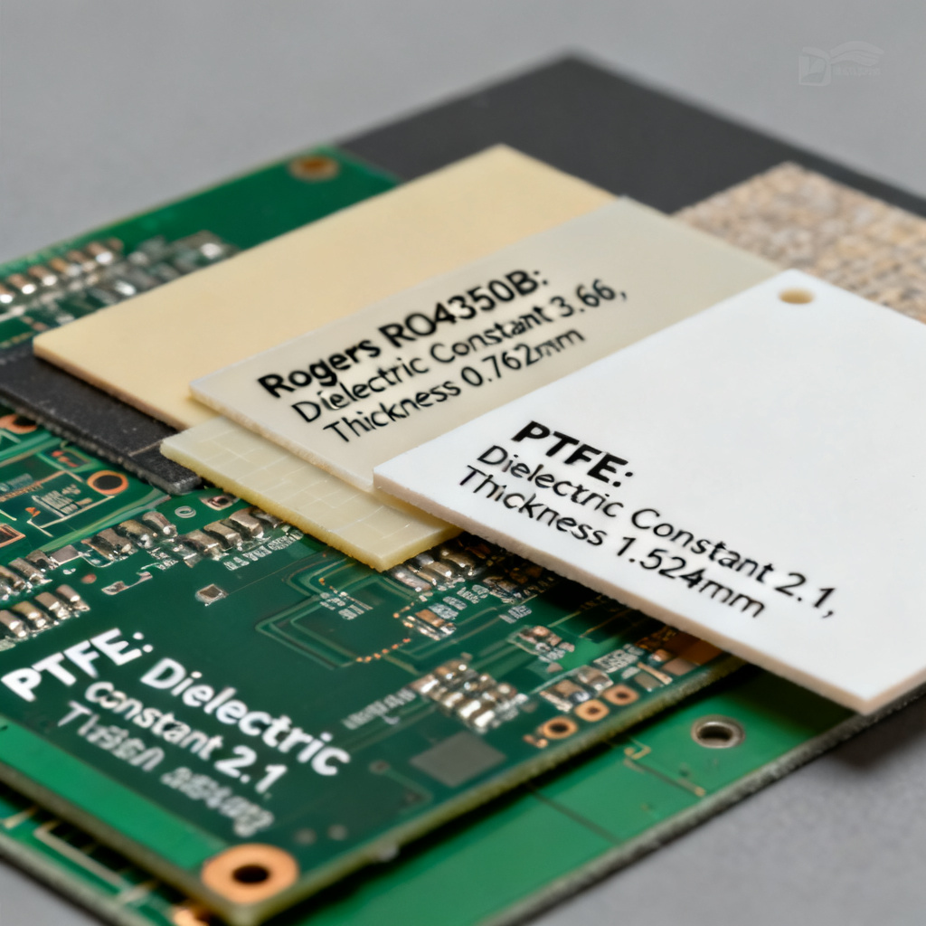
- Thermal Conductivity (k): The ability to dissipate heat. High-power RF circuits generate significant heat. Materials like ceramic-filled PTFE or hydrocarbon laminates (e.g., Rogers 4350B) offer higher thermal conductivity than pure PTFE.
- Moisture Absorption: Hygroscopic materials (like some standard FR-4) absorb moisture, which drastically changes Dk and Df at high frequencies. Low moisture absorption (< 0.02% by weight) is essential for stable RF performance.
1.2 Common High-Frequency Laminate Families
Based on the three authoritative guides, we categorize the most widely used materials for any high-frequency PCB guide:
| Material Family | Key Characteristics | Typical Applications | Example Products |
|---|---|---|---|
| PTFE / Woven Glass | Ultra-low Df, low moisture absorption, excellent high-frequency stability. Often soft and may require specialized handling (e.g., plasma etching). | Millimeter-wave, radar, satellite, high-end test equipment. | Rogers RT/duroid 5880, Taconic TLY-5 |
| Ceramic-Filled PTFE / Hydrocarbon | Lower cost than pure PTFE, better dimensional stability, good thermal conductivity. Df is low but slightly higher than pure PTFE. Dk is stable over temperature. | Base station antennas, power amplifiers, automotive radar (77 GHz). | Rogers RO3003, RO4350B; Isola Astra MT77 |
| High-Speed FR-4 / Modified Epoxy | A compromise for cost-sensitive high-speed digital (not pure RF). Df is moderate (0.005-0.015). Dk is somewhat stable. | High-speed digital backplanes, Gigabit Ethernet, PCIe Gen 3/4. | Isola FR408HR, Nelco N4000-13SI |
| Low Loss / Very Low Loss | A step above standard FR-4, often using PPE or PPO resins. Good for applications up to ~10 GHz. | 5G small cells, IoT modules, networking equipment. | Panasonic Megtron 6, TUC TU-872 SLK |
Expert Recommendation from Top Sources: For RF Power Amplifiers (1-10 GHz), Rogers RO4350B is the industry workhorse due to its balance of low loss, good thermal performance, and consistent Dk (3.48 at 10 GHz). It can be processed using standard FR-4 etching, reducing fabrication cost. For Millimeter-Wave (30-100 GHz), pure PTFE laminates like Rogers RT/duroid 5880 or Taconic TLY-5 are preferred for their ultra-low Df (0.0009) and stable Dk (2.20). For High-Speed Digital (10-28 Gbps), Megtron 6 or Isola Astra MT77 offer low Df and excellent signal integrity for very high-speed serial links.
1.3 Copper Foil Roughness and Surface Finish
At micro-wave and millimeter-wave frequencies, conductor losses are heavily dictated by the physical topography of the copper interface due to the Skin Effect.
- The Impact of Roughness: As frequency scales upward, electrical current restricts itself to the ultra-thin outer boundaries of the trace. Rough copper treatment increases the physical path length of the signal, drastically driving up resistive attenuation. Always specify Very Low Profile (VLP) or reverse-treated foils for high-frequency paths.
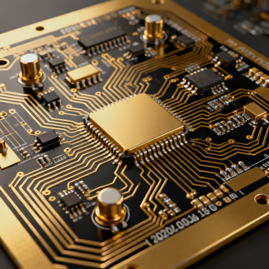
- Surface Finish Selection: Never deploy Hot Air Solder Leveling (HASL) due to its uneven thickness profile. Electroless Nickel Immersion Gold (ENIG) is the baseline standard for RF. For wire-bonding or tighter tolerances, opt for Immersion Silver or ENEPIG to eliminate nickel-induced losses.
2. Controlled Impedance and Transmission Lines
In any high-frequency PCB guide, the goal is to match the impedance of the source, the trace, and the load to minimize reflections and maximize power transfer.
2.1 The Concept of Characteristic Impedance (Z0)
Characteristic impedance is the ratio of voltage to current for a traveling wave on a transmission line. It is determined solely by the geometry of the trace and the properties of the surrounding dielectric, not by the length of the line. The standard impedance for most RF systems is 50 ohms (a compromise between power handling and loss). For digital systems, 50 ohms is common, but 75 ohms is used for video/cable TV.
2.2 Common Transmission Line Structures
Based on the compiled expert knowledge for this high-frequency PCB guide:
| Structure | Description | Impedance Formula (Simplified) | Key Considerations |
|---|---|---|---|
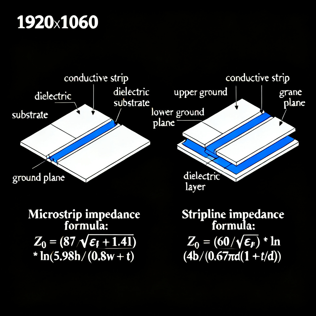
| Microstrip | A trace on the outer layer, with a ground plane beneath. | Z0 ≈ 87 / √(εr+1.41) * ln(5.98h / (0.8w+t)) | Most common for top/bottom layers. Easy to fabricate. Susceptible to external noise. |
| Stripline | A trace embedded between two ground planes, centered in the dielectric. | Z0 ≈ 60 / √εr * ln(4h / 0.67πw(0.8+t/w)) | Excellent isolation and EMI shielding. Used for high-density inner layers. |
| Coplanar Waveguide (CPW) | A trace with ground planes on the same layer, on both sides, with a gap. | More complex; requires field solvers. | Excellent for RF ICs and components with ground-signal-ground (GSG) pads. |
| Differential Pair | Two coupled traces carrying equal and opposite signals. | Zdiff ≈ 2 * Z0 (for edge-coupled) | Used for high-speed digital (USB, HDMI, PCIe). Common impedance is 100 ohms differential. |
2.3 Factors Affecting Impedance in PCB Fabrication
All three top sources emphasize that theoretical calculations must account for real-world manufacturing tolerances. The fabricator must control: Trace Width (w) – the most critical factor. A 0.5 mil variation can shift impedance by 2-3 ohms. Dielectric Height (h) – the thickness of the prepreg or core between the trace and the reference plane. Tolerances of ±10% are typical. Copper Thickness (t) – finished copper thickness (e.g., 1 oz = 1.4 mils). Etching undercut reduces the effective trace width. Dielectric Constant (εr) – as noted, it varies by frequency and material lot. Solder Mask – the presence of solder mask on outer layers effectively adds a thin layer of dielectric, lowering the impedance. For critical RF, specify solder mask over bare copper (SMOBC) or use a “solder mask defined” impedance calculation.
Actionable Best Practice: Provide the fabricator with target impedance (e.g., 50 ohms ±5%). Do not specify exact trace width and dielectric thickness. Instead, let the fabricator’s engineering team calculate the stackup based on their specific material tolerances and etching processes. Request impedance test coupons on the panel to verify actual impedance after fabrication.
3. RF Design and Layout Rules
This section integrates the most sophisticated layout strategies from the top-ranking guides, focusing on minimizing parasitic effects, crosstalk, and losses in your high-frequency PCB guide.
3.1 Grounding and Return Paths
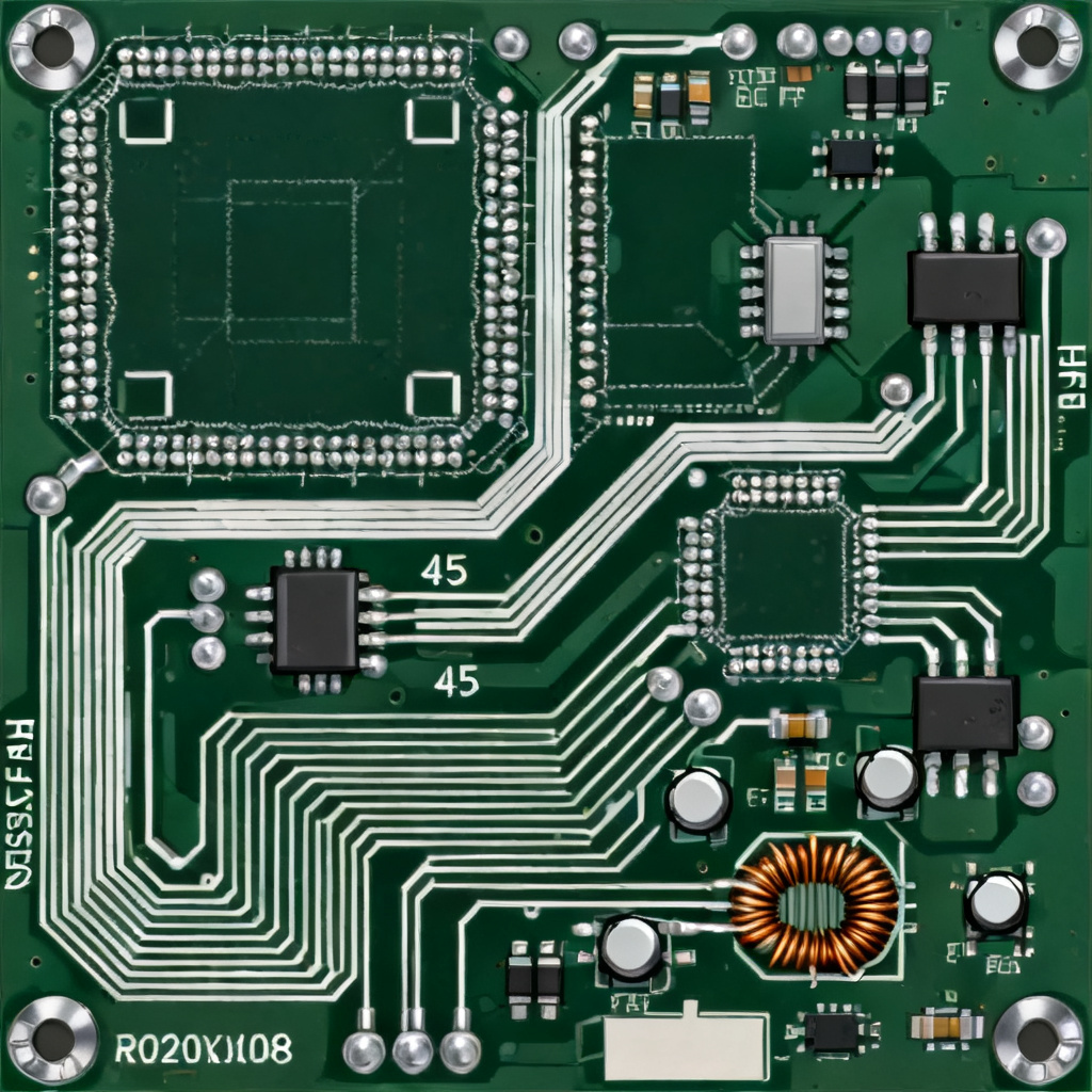
The golden rule of RF layout is simple: Every high-frequency signal trace must mirror a continuous, uninterrupted return path directly beneath it.
- Solid Ground Plane Integrity: Dedicate Layer 2 as a solid, unbroken reference ground. Never route an RF trace across an isolation split or plane gap, as doing so creates a massive inductive loop that destroys signal integrity and amplifies EMI.
- Via Stitching Guidelines: Place rows of grounding vias along the boundaries of RF transmission lines and the board perimeter to suppress parasitic parallel-plate waveguide modes.
📏Design Rule of Thumb: Space shielding vias at a maximum interval of (one-twentieth of the guided wavelength). For instance, a 2.4 GHzcircuit requires a strict maximum via spacing of 6mm to prevent the slot from behaving as an unwanted antenna.
3.2 Signal Routing Best Practices
Avoid 90-Degree Corners: While not catastrophic at low frequencies, at RF, a 90-degree corner creates a capacitance discontinuity and can radiate. Use 45-degree chamfered corners or curved traces. Minimize Via Count: Every via introduces an inductance (typically 0.5-1 nH) and a capacitance discontinuity. For critical RF paths, use a single via or a carefully tuned via transition. When a via is unavoidable, use back-drilling to remove the unused stub, which acts as a resonant element. Length Matching: For differential pairs and parallel buses (e.g., DDR memory), match trace lengths to within a few mils to ensure signals arrive simultaneously. Use serpentine routing with a pitch of at least 3x the trace width to minimize coupling. Keep Stubs Short: Any trace stub (a branch off the main signal path) acts as a capacitor or an open-circuit stub that reflects energy. The rule: keep any stub shorter than λ/10 of the highest frequency component. Ideally, use a “daisy chain” topology instead of “T” or “star” routing.
3.3 Component Placement and Decoupling
Placement Order: Arrange components in the signal flow direction (input to output) in a linear path. Avoid looping signals back over the input. Decoupling Capacitors: For RF, use low-ESR, low-ESL capacitors (e.g., 100 pF, 10 nF, 1 µF in parallel). Place them as close as possible to the power pin of the active device. The loop area from the capacitor to the IC pin and back to the ground plane must be minimized. Use multiple vias to connect the capacitor’s ground pad to the ground plane. Power Plane Isolation: For mixed-signal boards, use a dedicated power plane with a clean, isolated island for the RF section. Connect the RF power island to the main power supply through a ferrite bead or a pi-filter.
3.4 Thermal Management in RF Design
RF components, especially power amplifiers, generate significant heat. Poor thermal management degrades performance and reliability. Thermal Vias: Place a grid of small vias (e.g., 0.3 mm diameter) under the component’s thermal pad to conduct heat to the inner ground planes, which act as heat spreaders. Copper Pour: Use large copper pours on the top and bottom layers connected to the thermal vias. Avoid creating isolated copper islands (copper thieving) that are not connected to ground. Material Selection: As discussed in Part 1, materials with higher thermal conductivity (e.g., ceramic-filled laminates) help dissipate heat.
4. Simulation, Testing, and Manufacturing Considerations
This final section of the high-frequency PCB guide covers verification and production aspects.
4.1 The Role of 3D EM Simulation
All three expert sources agree: for frequencies above 1 GHz, hand calculations are insufficient. Use 3D electromagnetic (EM) field solvers (e.g., Ansys HFSS, Keysight ADS, CST Studio Suite) to model complex structures like via transitions, connectors, and filter sections; simulate S-parameters, impedance, and coupling; and validate the design before fabrication, reducing costly prototype spins.
4.2 Fabrication Tolerances and DFM
Minimum Trace/Spacing: For standard RF (up to 10 GHz), 4/4 mil (0.1 mm) is achievable. For millimeter-wave, 3/3 mil or finer is required, which increases cost. Registration: For multilayer boards with tight impedance control, ensure the fabricator has tight layer-to-layer registration tolerances (e.g., ±5 mils). Material Certification: Request that the laminate supplier provides a Dk and Df test report for the specific lot used in your order. This is a standard service from Rogers and Taconic.
4.3 Testing and Verification
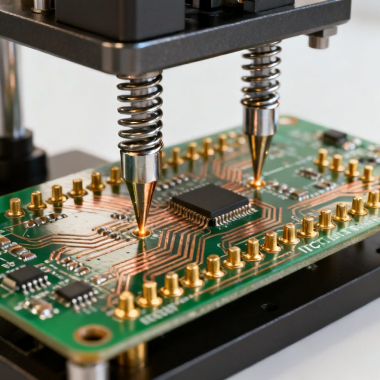
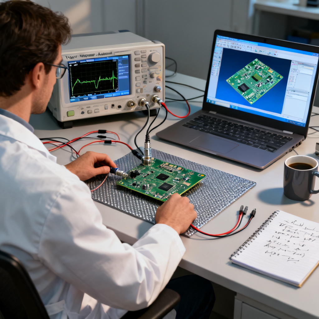
TDR (Time Domain Reflectometry): Used to measure impedance profiles along a trace. It can pinpoint discontinuities like vias, connectors, or impedance mismatches. VNA (Vector Network Analyzer): Used to measure S-parameters (return loss, insertion loss, isolation) over a frequency range. This is the gold standard for RF performance validation. Flying Probe vs. Bed of Nails: For RF boards, flying probe testing is preferred to avoid the parasitic effects of a custom test fixture.
5. Conclusion: A Holistic Approach to High-Frequency PCB Success
Designing a successful high-frequency PCB is not a single-step task; it is a holistic process that integrates material science, transmission line theory, and meticulous layout practices. By understanding the trade-offs between material types (PTFE vs. hydrocarbon vs. high-speed FR-4), mastering impedance control (50 ohms, 100 ohms differential), and applying rigorous layout rules (solid ground planes, minimized vias, proper decoupling), you can achieve first-pass success.
For the B2B buyer, this high-frequency PCB guide serves as a specification tool. When sourcing a high-frequency PCB, you must communicate: target impedance and tolerance; operating frequency and loss budget; required material (e.g., Rogers RO4350B or equivalent); layer stackup (e.g., 4-layer, 1 oz copper, 0.062″ total thickness); and surface finish (ENIG) and copper foil profile (VLP). By partnering with a fabricator that understands these nuances—and by using this guide as your technical reference—you ensure that your high-frequency designs perform reliably in the field, delivering the signal integrity and power efficiency your applications demand.
This guide is a living document. For specific stackup calculations or material recommendations for your project, please contact our engineering team. We specialize in high-frequency PCB fabrication and can provide free DFM feedback on your design files.
6. Frequently Asked Questions about High-Frequency PCB Design
What is the best material for a high-frequency PCB?
For most applications in a high-frequency PCB guide, Rogers RO4350B is recommended for its balance of low loss, thermal performance, and consistent Dk. For millimeter-wave designs, PTFE-based laminates like Rogers RT/duroid 5880 are preferred.
How do I control impedance in high-frequency PCB design?
Controlled impedance in a high-frequency PCB guide is achieved by selecting the correct trace width, dielectric height, and copper thickness. Use microstrip or stripline structures and always specify target impedance to your fabricator.
Why is FR-4 not suitable for high-frequency PCBs?
FR-4 has a high dissipation factor (Df) and inconsistent dielectric constant (Dk) at frequencies above 1 GHz, leading to significant signal loss and impedance variation. This high-frequency PCB guide recommends using low-loss laminates like Rogers or Isola materials.
What is the difference between microstrip and stripline in RF design?
Microstrip is on the outer layer with a single ground plane, while stripline is embedded between two ground planes. Stripline offers better isolation and is preferred for high-density designs, as detailed in this high-frequency PCB guide.
How do I reduce signal loss in a high-frequency PCB?
To reduce loss in a high-frequency PCB guide, use low-Df materials, VLP copper foil, minimize via count, avoid 90-degree corners, and ensure proper impedance matching. Also, use ENIG surface finish and back-drilling for critical paths.