PCB Grounding Strategies Single Point Multi Point and Mixed
This comprehensive technical guide focuses on PCB Grounding Strategies Single Point Multi Point and Mixed design for hardware engineers. In printed circuit board layouts, selecting the correct grounding approach is the most critical factor for electromagnetic compatibility (EMC), signal integrity, and system reliability. This manual explores their principles, applications, advantages, and best practices.
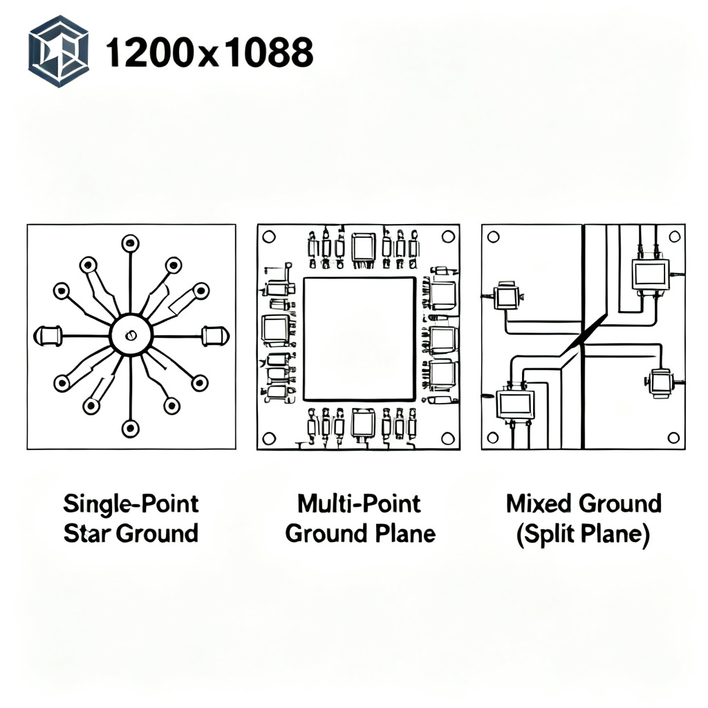
Core Concepts of PCB Grounding Strategies
Understanding PCB grounding strategies starts with grasping ground planes, ground loops, and impedance-frequency relationships. A ground plane is a large copper area providing low-impedance return paths and stable reference voltage. It offers low impedance, shielding, and signal integrity. A ground loop occurs with multiple ground paths, inducing noise. At low frequencies, resistance dominates; at high frequencies, inductive reactance requires multi-point grounding.
What is a Ground Plane?
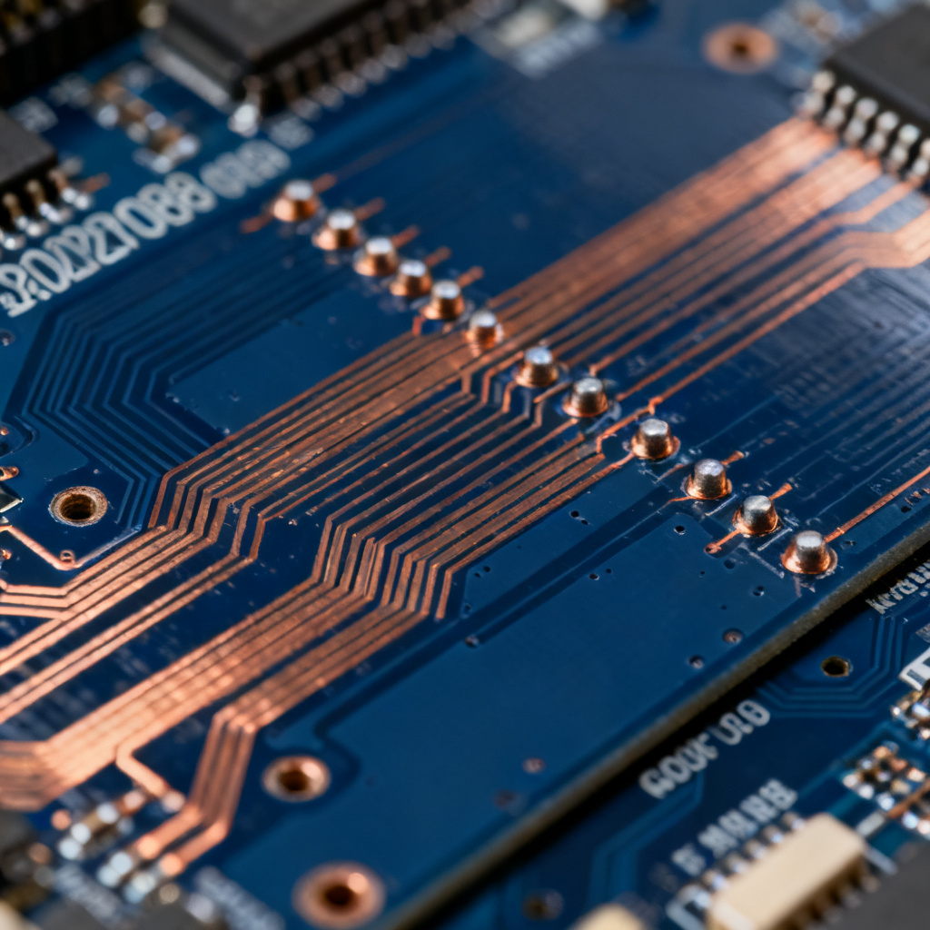
A ground plane is a continuous copper layer in multi-layer PCBs that minimizes resistance and inductance. PCB grounding strategies rely on this for high-frequency performance. Key benefits include low impedance, shielding against EMI, and stable reference for all components.
Ground Loops and Mitigation
Ground loops create voltage differences and noise. PCB grounding strategies mitigate loops via single-point grounding for low-frequency or low-impedance planes for high-frequency circuits. This is essential for signal integrity.
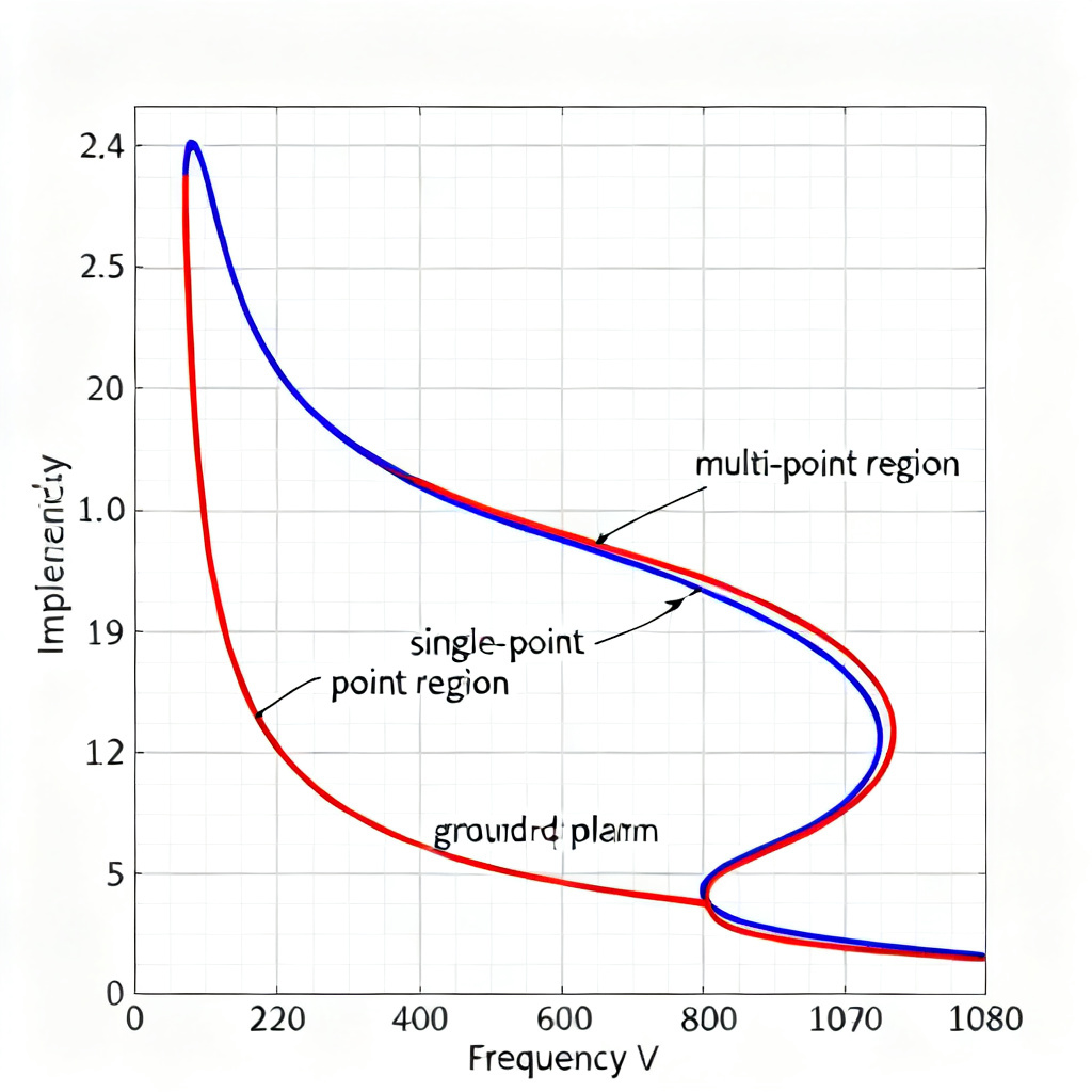
Impedance and Frequency Relationship
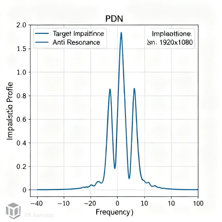
At frequencies below 1 MHz, single-point grounding works; above 10 MHz, multi-point is needed. Between 1–10 MHz, mixed grounding is ideal. PCB grounding strategies must match the frequency domain.
Single-Point Grounding: Low-Frequency Simplicity
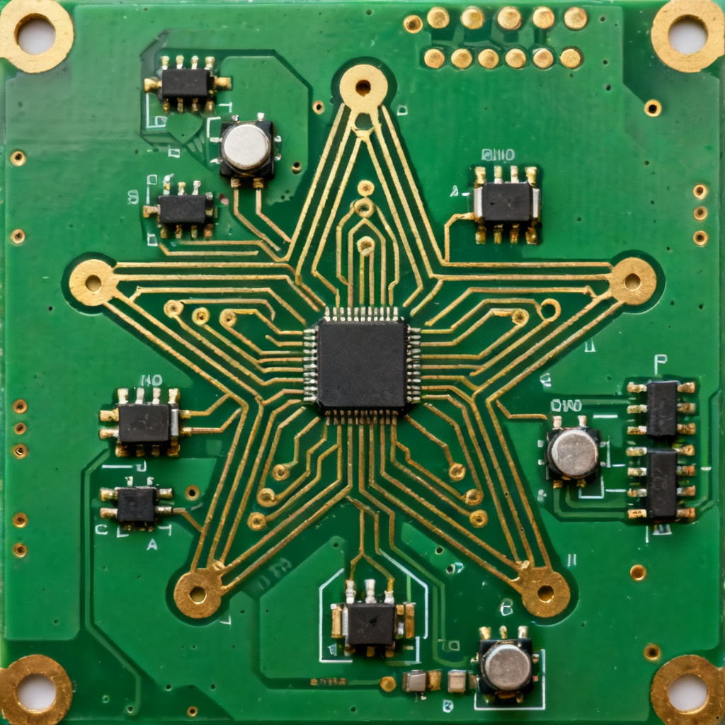
Single-point grounding connects all grounds to one physical point, ideal for low-frequency analog circuits. PCB grounding strategies include series and parallel configurations. Parallel single-point grounding eliminates shared impedance, often using star-grounding for each functional block.
Advantages of Single-Point Grounding
- Eliminates ground loops, critical for audio amplifiers and sensors.
- Simple design, cost-effective for low-complexity boards.
- Minimizes noise in precision measurement devices.
Limitations and Best Practices
Not suitable above 1 MHz due to trace inductance. PCB grounding strategies recommend parallel grounding, short wide traces, and strategic single-point placement near power supply. Separate analog and digital grounds until the single point.
Multi-Point Grounding: High-Frequency Solution
Multi-point grounding connects all grounds to a low-impedance ground plane, standard for high-speed digital and RF circuits. PCB grounding strategies use a continuous plane to minimize loop area and inductance.
Advantages of Multi-Point Grounding
- Low inductance, nanohenry range, essential for high-speed signals like DDR and USB.
- Excellent EMI performance, simplifying compliance.
- Simplifies routing with ground plane always nearby.
Limitations and Best Practices
Risk of ground loops in multi-board systems. Use dedicated ground plane layer, multiple vias, avoid slots, and add ground stitching. PCB grounding strategies require careful partitioning for mixed-signal designs.
Mixed Grounding: Hybrid Approach for Mixed-Signal
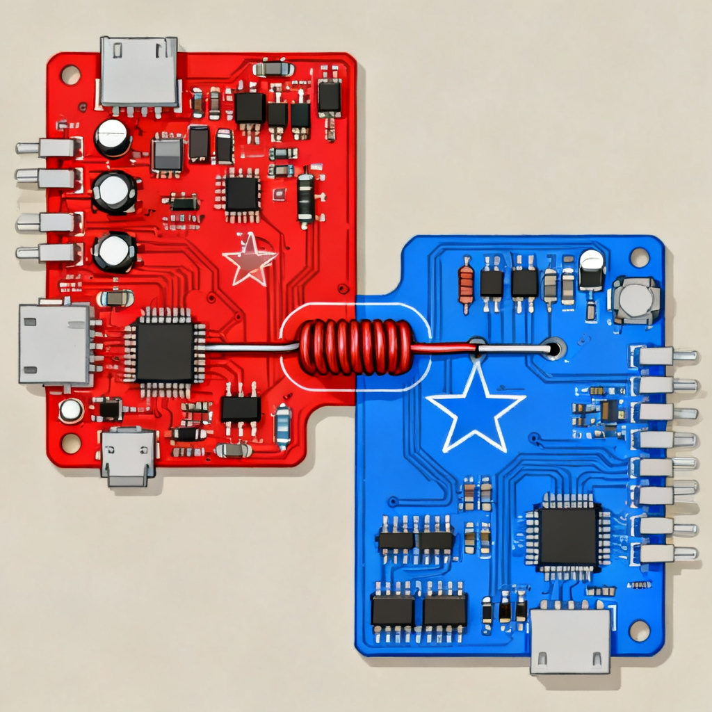
Mixed grounding combines single-point and multi-point techniques for mixed-signal circuits. PCB grounding strategies divide the board into analog (single-point) and digital (multi-point) domains, connected at one point near the mixed-signal device.
Advantages of Mixed Grounding
- Prevents digital noise corrupting analog signals.
- Flexibility for complex designs with wide frequency range.
- Improved EMC through isolation.
Best Practices for Mixed Grounding
Use a solid ground plane with physical separation, connect analog and digital grounds at the ADC/DAC, use ferrite beads or zero-ohm resistors, and keep digital traces away from analog areas. PCB grounding strategies benefit from isolation techniques for extreme cases.
Advanced Grounding Techniques
Advanced PCB grounding strategies include EMC compliance via solid planes and stitching vias, high-speed digital grounding for impedance control, RF grounding with via fences, and power electronics grounding with thick copper and Kelvin connections.
Grounding for EMC Compliance
Use solid ground plane, route high-speed traces over it, and add ferrite beads for decoupling. PCB grounding strategies minimize radiated emissions.
Grounding for High-Speed Digital
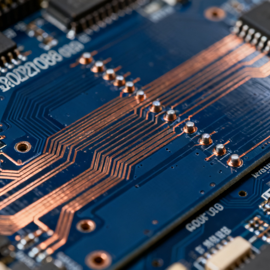
Maintain 50-ohm impedance, use differential pairs, and avoid ground plane cutouts. PCB grounding strategies ensure signal integrity for DDR, PCIe, and USB.
Grounding for RF Circuits
Use grounded coplanar waveguide, via fences, and microstrip/stripline structures. PCB grounding strategies provide controlled impedance and isolation.
Grounding for Power Electronics
Use thick copper, separate power and signal grounds, and implement Kelvin connections. PCB grounding strategies handle high currents and fast switching.
Common Grounding Mistakes
| Mistake | Problem | Solution in PCB Grounding Strategies |
|---|---|---|
| Single plane without partitioning | Digital noise contaminates analog | Physically separate components, use solid plane |
| Multiple ground points create loops | Hum and interference | Single-point for low-frequency, low-impedance plane |
| High-speed traces over slots | Large loop area, increased EMI | Avoid slots, use stitching capacitors |
| Ignoring via inductance | Degraded high-frequency performance | Use multiple parallel vias |
| Star ground with long traces for high-frequency | Ineffective above 1 MHz | Use ground plane instead |
Practical Implementation Guide
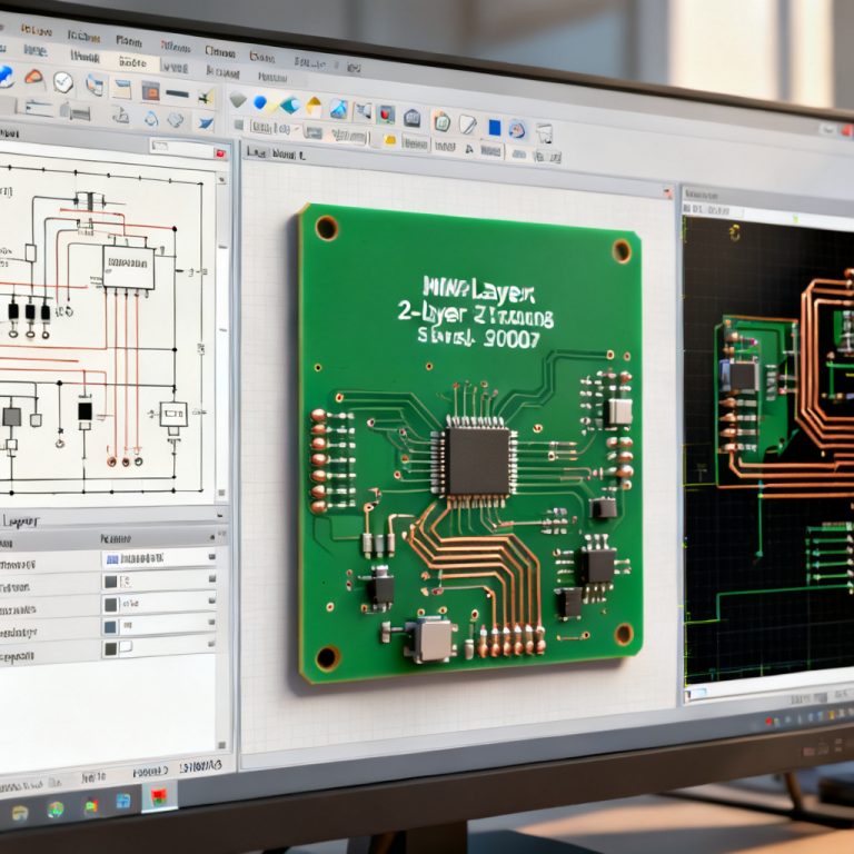
Apply PCB grounding strategies step-by-step: analyze frequency range, choose layer stackup (2-layer to 6+ layers), partition board physically, design ground system, and verify with simulation and testing.
Step 1: Analyze Circuit Frequency
Low-frequency analog (<1 MHz): single-point. High-frequency digital (>10 MHz): multi-point. Mixed-signal: mixed grounding.
Step 2: Choose Layer Stackup
2-layer: ground plane on bottom. 4-layer: dedicated ground and power planes. 6+ layers: multiple ground planes for low impedance.
Step 3: Partition Board
Place analog and digital components separately, keep high-speed traces away from analog inputs, use guard traces.
Step 4: Design Ground System
Single-point: star ground near power supply. Multi-point: continuous plane. Mixed: connect domains at mixed-signal device.
Step 5: Verify
Use EMC simulation tools, test for loops and noise with oscilloscope or spectrum analyzer.
FAQ: PCB Grounding Strategies
What is the best PCB grounding strategy for low-frequency analog circuits?
Single-point grounding is best for low-frequency analog circuits, as it eliminates ground loops and minimizes noise in audio amplifiers and sensors.
How does multi-point grounding improve high-speed digital design?
Multi-point grounding provides a low-impedance ground plane, reducing inductance and EMI for high-speed signals like DDR and USB.
When should I use mixed grounding?
Mixed grounding is ideal for mixed-signal circuits with both analog and digital components, preventing noise coupling while maintaining high-frequency performance.
What is a ground loop and how do PCB grounding strategies prevent it?
A ground loop is a closed path for ground currents that induces noise. Single-point grounding prevents loops by providing a single return path.
Can I use a single ground plane for all circuits?
Yes, but careful physical separation of analog and digital components is required to avoid noise contamination. Mixed grounding may be better for sensitive designs.
Conclusion: Choosing the Right Strategy
PCB grounding strategies are not one-size-fits-all. Single-point grounding suits low-frequency analog, multi-point for high-speed digital/RF, and mixed for complex mixed-signal systems. At [Your Company Name], we specialize in PCB production and customization for export, from prototype to high-volume manufacturing. Our experts help design optimized grounding for signal integrity and EMC compliance. Contact us today for your next project.