Power Integrity in PCB Design PDN Decoupling Ripple
This comprehensive technical manual focuses on Power Integrity in PCB Design PDN Decoupling Ripple analysis. Mastering Power Integrity in PCB Design is non-negotiable for modern high-speed, high-reliability applications. This guide provides an exhaustive, expert-level overview of Power Distribution Networks (PDNs), decoupling capacitor strategies, and ripple suppression, ensuring your board delivers clean, stable power to every active component.
Why Power Integrity Matters
In the era of sub-1V core voltages and multi-GHz switching speeds, Power Integrity in PCB Design has become as critical as Signal Integrity (SI). A poorly designed power distribution network can lead to voltage droops, excessive ripple, electromagnetic interference (EMI), and functional failures. Unlike SI, which deals with signal paths, PI focuses on delivering a constant, low-impedance voltage from the regulator to every load—across all frequencies. The three key pillars of PI are: PDN Impedance, Decoupling, and Ripple & Noise.
PDN Design & Analysis: What is a PDN?
A PDN comprises all elements from the voltage regulator module (VRM) to the IC power pins: VRM, bulk capacitors, PCB planes (power and ground), vias, traces, and decoupling capacitors. Its primary role is to maintain a stable voltage within the specified tolerance (e.g., ±3% for a 1.0V core).
Target Impedance: The Golden Rule
The most fundamental PI design goal is achieving a target impedance (Z_target) across the frequency range of interest. This is calculated as: Z_target = (VDD × Tolerance) / I_transient. For a 1.0V rail with 3% tolerance and 10A transient, Z_target = (1.0 × 0.03) / 10 = 3 mΩ. This impedance must be maintained from DC up to the highest frequency of interest (often 1 GHz or more).
PDN Impedance Profile: The Key Metric
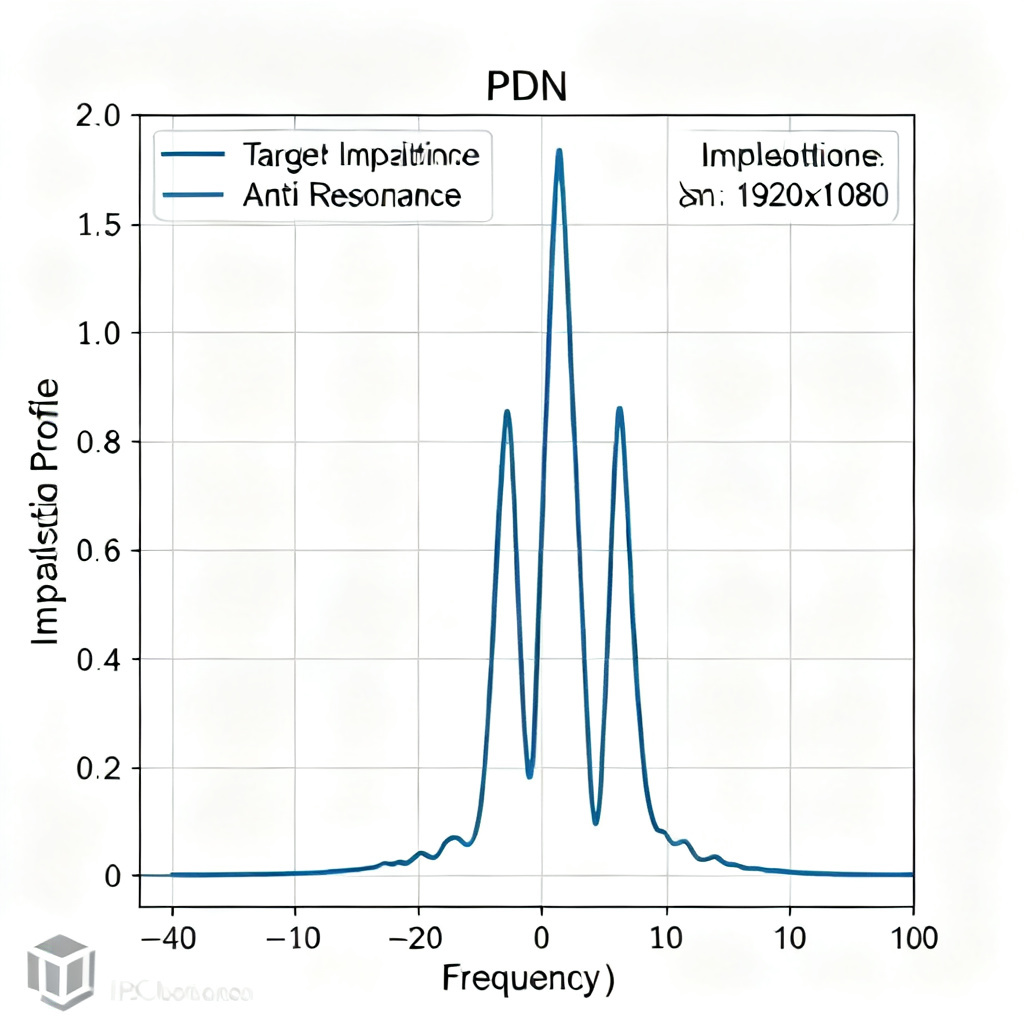
A PDN’s impedance profile is a plot of impedance vs. frequency. Ideally, it should be flat and below Z_target. In reality, it exhibits peaks and valleys due to resonances between board capacitance, package inductance, and discrete capacitors. The most critical resonance is the anti-resonance—a high-impedance spike where the inductive and capacitive reactances cancel.
This occurs between the VRM’s output inductance and the first bulk capacitor, or between different capacitor types. How to read an impedance profile: Low frequencies (DC to ~10 kHz) dominated by VRM output impedance; Mid frequencies (10 kHz to ~10 MHz) shaped by bulk tantalum/polymer and ceramic capacitors; High frequencies (10 MHz to 1 GHz) governed by small-value MLCCs, PCB plane capacitance, and IC package parasitics; Above 1 GHz entirely dependent on on-die capacitance.
VRM Role in PDN
The VRM (e.g., buck converter) is the source. Its output impedance is typically inductive at high frequencies. A fast, well-designed VRM reduces low-frequency impedance but cannot handle high-frequency transients. Thus, the VRM’s bandwidth (typically 10–100 kHz) defines the low-frequency cutoff for decoupling.
PCB Plane Capacitance
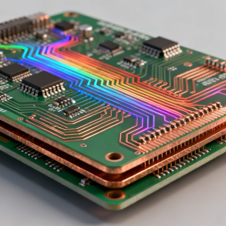
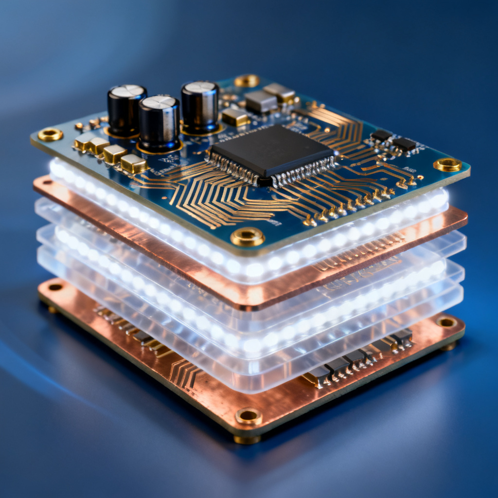
The power and ground planes form a parallel-plate capacitor. This distributed capacitance is a critical high-frequency decoupling element because it has extremely low ESL (effective series inductance). To maximize plane capacitance: Use thin dielectric between power and ground layers (e.g., 2–4 mils for high-speed designs); Avoid splitting planes unnecessarily; Keep a continuous reference plane; Place power and ground layers adjacent to each other (stack-up: Signal-Ground-Power-Signal). The plane capacitance per square inch is: C = (ε0 × εr × Area) / Distance. For FR4 (εr ≈ 4.5), a 4 mil gap gives ~225 pF/in². This is invaluable for frequencies above 50 MHz.
Decoupling Capacitor Strategy
Why Decoupling?
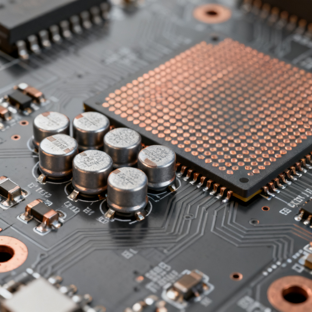
Decoupling capacitors act as local energy reservoirs. They provide instantaneous current during switching events, bypassing the inductance of the PDN. Without them, voltage droop would exceed tolerance. The goal is to create a low-impedance path from the capacitor to the IC power pin across all frequencies.
Capacitor Physics: ESL, ESR, and SRF
Every real capacitor has parasitic resistance (ESR) and inductance (ESL). The Self-Resonant Frequency (SRF) is where the capacitor’s capacitance and ESL resonate, creating minimum impedance. Above SRF, the capacitor becomes inductive and loses effectiveness. SRF = 1 / (2π √(L × C)). For a 100 nF MLCC with 0.5 nH ESL, SRF ≈ 22.5 MHz. For a 10 nF MLCC with 0.5 nH ESL, SRF ≈ 71 MHz. Key rule: Use different capacitor values to cover a wide frequency range. Typically, a geometric cascade (e.g., 10 µF, 1 µF, 0.1 µF, 0.01 µF) spaced by a factor of 10–100 in value ensures overlapping impedance minima.
Types of Capacitors for PDN Decoupling
Bulk Capacitors (Electrolytic, Tantalum, Polymer): High capacitance (1–1000 µF), high ESR, high ESL. Used for low-frequency decoupling (1 kHz–1 MHz). Polymer capacitors offer lower ESR than tantalum. MLCCs (Multilayer Ceramic Capacitors): Low ESL (down to 0.1 nH for 0201 packages), low ESR, high SRF. Ideal for mid-to-high frequencies (1 MHz–1 GHz). X7R and X5R dielectrics offer high capacitance density; NP0/C0G offers better stability. Embedded Capacitance: Thin laminate layers with high dielectric constant (e.g., 10–20 µF/in²) embedded in the PCB. This is the ultimate high-frequency decoupling, eliminating via inductance.
The Anti-Resonance Problem
When two capacitor values with different SRFs are placed in parallel, their impedance curves intersect, creating an anti-resonance peak at the frequency where the lower-value capacitor is inductive and the higher-value is capacitive. This peak can exceed Z_target. Mitigation strategies: Use capacitors with similar ESL but different C values; Add a small resistor (e.g., 0.1–1 Ω) in series with one capacitor to dampen the peak (though this increases ESR); Use a “spread” of values with overlapping impedance curves (e.g., 4.7 µF, 2.2 µF, 1.0 µF, 0.47 µF) rather than decade steps; Simulate the impedance profile with tools like Keysight ADS, Ansys SIwave, or Altium PDN Analyzer.
Placement & Mounting Inductance
The total inductance of a decoupling capacitor includes its package ESL plus the inductance of vias, traces, and pads. This mounting inductance can be 2–5 nH for a standard via, dwarfing the capacitor’s own ESL.
Best practices for minimizing mounting inductance: Place capacitors as close as possible to the IC power pins (within 50–100 mils for high-speed); Use micro-vias or through-hole vias directly adjacent to capacitor pads (avoid long traces); Connect capacitors to the power and ground planes via multiple vias in parallel (e.g., 2–4 vias per capacitor) to reduce inductance; For BGA packages, place capacitors on the backside directly under the BGA, or use buried capacitors in inner layers; Use smaller package sizes (0402, 0201) to reduce ESL.
How Many Capacitors Do You Need?
The number of capacitors depends on the transient current and the target impedance. A common rule of thumb: use one bulk capacitor per voltage rail (e.g., 10–100 µF) and one high-frequency MLCC per power pin of the IC. For high-current ASICs, this can mean 10–50 MLCCs. However, simulation is essential. A simple spreadsheet calculation often underestimates the number needed due to anti-resonances and mounting inductance.
Ripple & Noise:What is Ripple?
Ripple is the periodic AC component on the DC output of a power supply, typically at the switching frequency (e.g., 500 kHz for a buck converter) and its harmonics. Noise includes random fluctuations and coupled interference from neighboring signals.
Sources of Ripple in PDN
Switching Regulator: Output ripple due to inductor current ripple and output capacitor ESR. Typical ripple voltage = I_ripple × ESR_out. Load Transients: Sudden current changes cause voltage droops (undershoot) and overshoots. Simultaneous Switching Noise (SSN): When many outputs switch simultaneously, they draw a large current spike, causing a voltage dip on the power rail (ground bounce). Crosstalk: Noise from adjacent signal traces couples into the power plane.
Measuring Ripple & Noise
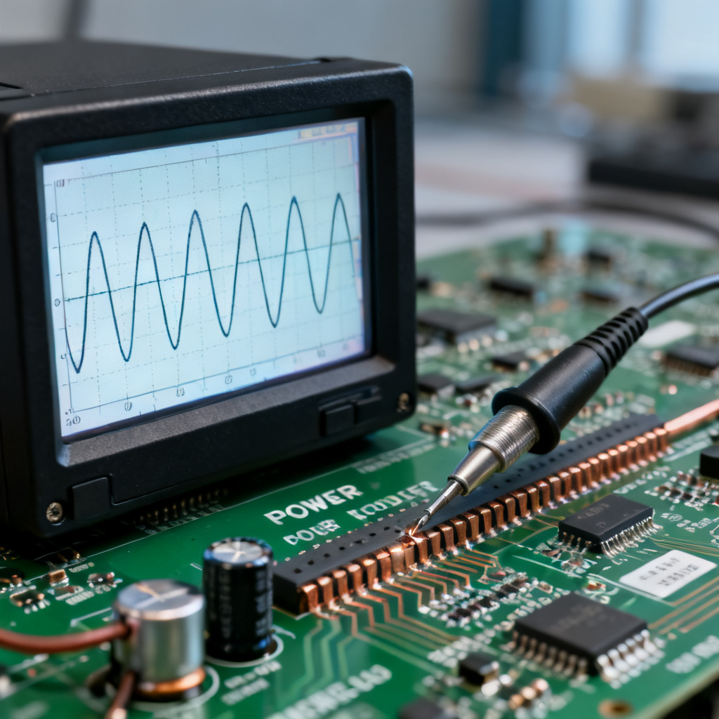
Use a 1:1 probe or a coaxial cable with AC coupling to avoid DC offset. Set the oscilloscope bandwidth to 20 MHz (standard for ripple measurement) or full bandwidth (for noise). Measure at the IC power pin using a small loop (minimize probe ground lead inductance). Typical acceptable ripple: < 1% of VDD for digital, < 0.1% for analog/RF.
Ripple Mitigation Techniques
Output Filter: Add an LC filter (ferrite bead + capacitor) after the VRM to attenuate switching ripple. Choose a ferrite bead with high impedance at the switching frequency. Spread Spectrum: Some VRMs support spread-spectrum modulation to reduce peak ripple amplitude at the cost of wider bandwidth. Star Point Routing: For mixed-signal designs, separate analog and digital power planes and connect them at a single point (star point) to prevent digital noise from contaminating analog supplies. Guard Rings: Surround sensitive analog blocks with a grounded copper ring to isolate them from digital noise.
Ground Bounce & Simultaneous Switching Noise (SSN)
SSN occurs when many outputs switch simultaneously, causing a voltage drop across the ground inductance. This is especially severe in high-speed buses (DDR, PCIe). Mitigation: Use multiple ground vias per signal via to reduce ground inductance; Place decoupling capacitors close to the switching I/O banks; Use low-inductance packages (e.g., BGA with power/ground in the center).
Practical PDN Design Flow
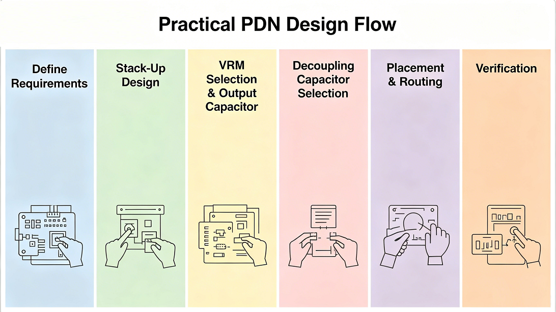
Step 1: Define Requirements
Determine VDD, tolerance, I_transient, and Z_target for each rail. Identify highest frequency of interest (usually 1/10 of the rise time: f_max = 0.35 / t_rise).
Step 2: Stack-Up Design
Place power and ground layers adjacent. Use thin dielectric (2–4 mils) for high-frequency rails. Assign dedicated plane layers for each major voltage (e.g., 1.0V, 1.8V, 3.3V).
Step 3: VRM Selection & Output Capacitor
Choose a VRM with bandwidth > 10× the transient frequency. Select output bulk capacitors (e.g., 4 × 47 µF polymer) to meet low-frequency impedance.
Step 4: Decoupling Capacitor Selection
Use simulation (e.g., Altium PDN Analyzer, Ansys SIwave, or Cadence Sigrity) to find the optimal capacitor count and values. Start with a “capacitor bank” approach: 1–2 bulk caps (10–100 µF) + 4–8 MLCCs (0.1–10 µF) per rail. Simulate impedance profile to ensure it stays below Z_target up to 1 GHz.
Step 5: Placement & Routing
Place decoupling caps within 100 mils of IC power pins. Use multiple vias per capacitor (2–4 vias). Avoid routing high-speed signals over split power planes.
Step 6: Verification
Perform DC IR drop analysis (voltage drop across planes due to resistance). Perform AC impedance simulation. Measure prototype using a vector network analyzer (VNA) or time-domain reflectometer (TDR) for PDN impedance.
Common Pitfalls & How to Avoid Them
Below is a summary of typical power integrity implementation risks and technical solutions:
| Pitfall | Consequence | Solution |
|---|---|---|
| Using only one capacitor value | Anti-resonance peaks above Z_target | Use a spread of values (e.g., 10 µF, 1 µF, 0.1 µF, 0.01 µF) |
| Placing capacitors far from IC | High mounting inductance negates capacitor effect | Place within 50–100 mils; use backside caps for BGA |
| Ignoring plane inductance | High impedance at high frequencies | Use thin dielectric; minimize plane loop area |
| Overlooking VRM bandwidth | Low-frequency decoupling insufficient | Ensure VRM bandwidth covers transient frequencies |
| Not simulating | Surprises during prototype testing | Simulate early and often; use free tools if needed |
Advanced Topics
Power Integrity for DDR Memory
DDR4/DDR5 requires extremely tight voltage tolerance (±2% for VDDQ). Use VTT termination and VREF planes with dedicated decoupling. Place decoupling caps on both sides of the DIMM connector.
Power Integrity for RF & Analog
Analog circuits (ADCs, PLLs) are sensitive to ripple above -80 dBc. Use LDOs after switching regulators for clean analog rails. Implement pi-filters (ferrite bead + cap + cap) on analog power inputs.
Using Simulation Tools
Free: LTSpice (for VRM and decoupling), Saturn PCB Toolkit (for trace resistance). Professional: Altium PDN Analyzer, Cadence Sigrity, Ansys SIwave, Keysight ADS. Online: Power Integrity calculators from Samtec, Murata, or TDK.
Conclusion & Call to Action
Power Integrity in PCB Design is not an afterthought—it is a foundational design discipline. By mastering PDN impedance, decoupling strategies, and ripple mitigation, you ensure your PCB delivers reliable performance from DC to GHz frequencies. Need expert PCB fabrication that supports your PI goals? Our advanced manufacturing capabilities include: Tight impedance control (±5%), Thin core dielectrics (2 mils), Embedded capacitance laminates, and Low-inductance via technologies. Contact us today for a free design review and quote. Let’s build power-optimized boards together.
Frequently Asked Questions
What is the target impedance in Power Integrity in PCB Design?
The target impedance (Z_target) is the maximum allowable impedance of the PDN to maintain voltage within tolerance. It is calculated as Z_target = (VDD × Tolerance) / I_transient. For example, a 1.0V rail with 3% tolerance and 10A transient requires Z_target of 3 mΩ.
How do decoupling capacitors improve Power Integrity in PCB Design?
Decoupling capacitors act as local energy reservoirs that provide instantaneous current during switching events, bypassing PDN inductance. They lower the impedance at specific frequency ranges, preventing voltage droop and maintaining stable power delivery.
What is the best way to minimize ripple in a PCB PDN?
Minimizing ripple involves using output LC filters, spread-spectrum VRMs, star-point routing for mixed-signal designs, and guard rings for sensitive analog blocks. Proper decoupling capacitor placement and simulation are also essential.
Why is Power Integrity in PCB Design critical for high-speed digital circuits?
High-speed digital circuits operate at sub-1V voltages with fast transient currents. Without proper PI, voltage droops and noise can cause timing violations, data errors, and EMI, leading to functional failures.