Green PCB Manufacturing: RoHS, REACH, Halogen‑Free & E‑waste
Welcome to the Green PCB Manufacturing RoHS REACH Halogen Free E waste comprehensive guide, the definitive industry resource for sustainable electronics. Adopting eco-friendly production ensures strict compliance, reduces environmental toxicity, and meets the global demand for green hardware.
The electronics industry relies on printed circuit boards (PCBs), and adopting green practices ensures compliance, reduces toxicity, and meets global demand for eco‑friendly production.RoHS Compliance | REACH Regulation | Halogen‑Free Materials | E‑waste Management | FAQ
RoHS Compliance: Eliminating Hazardous Substances in Green PCB Manufacturing
What is RoHS?
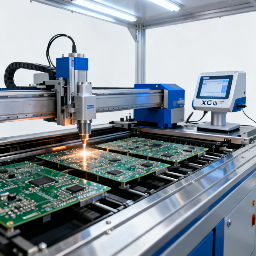
The Restriction of Hazardous Substances (RoHS) directive, originally adopted by the European Union in 2003 (Directive 2002/95/EC) and updated as RoHS 2 (2011/65/EU) and RoHS 3 (2015/863), limits the use of six (now ten) hazardous substances in electrical and electronic equipment. The original six substances are lead (Pb), mercury (Hg), cadmium (Cd), hexavalent chromium (Cr6+), polybrominated biphenyls (PBB), and polybrominated diphenyl ethers (PBDE). RoHS 3 added four phthalates: bis(2‑ethylhexyl) phthalate (DEHP), butyl benzyl phthalate (BBP), dibutyl phthalate (DBP), and diisobutyl phthalate (DIBP).
Impact on PCB Manufacturing
For PCBs, RoHS primarily affects solder, surface finishes, and laminates. Traditional lead‑based solder (e.g., Sn63Pb37) is replaced with lead‑free alternatives such as SAC alloys (tin‑silver‑copper, e.g., SAC305). Surface finishes like HASL (Hot Air Solder Leveling) have transitioned from lead‑based to lead‑free versions (e.g., ENIG, OSP, Immersion Silver). Laminate materials must avoid brominated flame retardants (PBBs and PBDEs). Compliance requires rigorous testing, including X‑ray fluorescence (XRF) analysis, to verify substance limits.
Benefits and Challenges
Benefits include reduced toxicity in manufacturing and end‑of‑life disposal, improved worker safety, and market access to EU and other regulated regions. Challenges include higher processing temperatures for lead‑free solder (requiring more energy and robust substrates), potential reliability issues (e.g., tin whiskers), and increased cost for alternative materials.
REACH Regulation: Managing Chemical Risks in Green PCB Manufacturing
Understanding REACH
REACH (Registration, Evaluation, Authorisation and Restriction of Chemicals) is an EU regulation (EC 1907/2006) that governs the production and use of chemical substances. Unlike RoHS, which restricts specific substances in finished products, REACH requires manufacturers to register all chemicals used in production, evaluate their risks, and obtain authorization for substances of very high concern (SVHCs). The SVHC list is updated regularly, with over 200 substances currently listed.
REACH in PCB Manufacturing
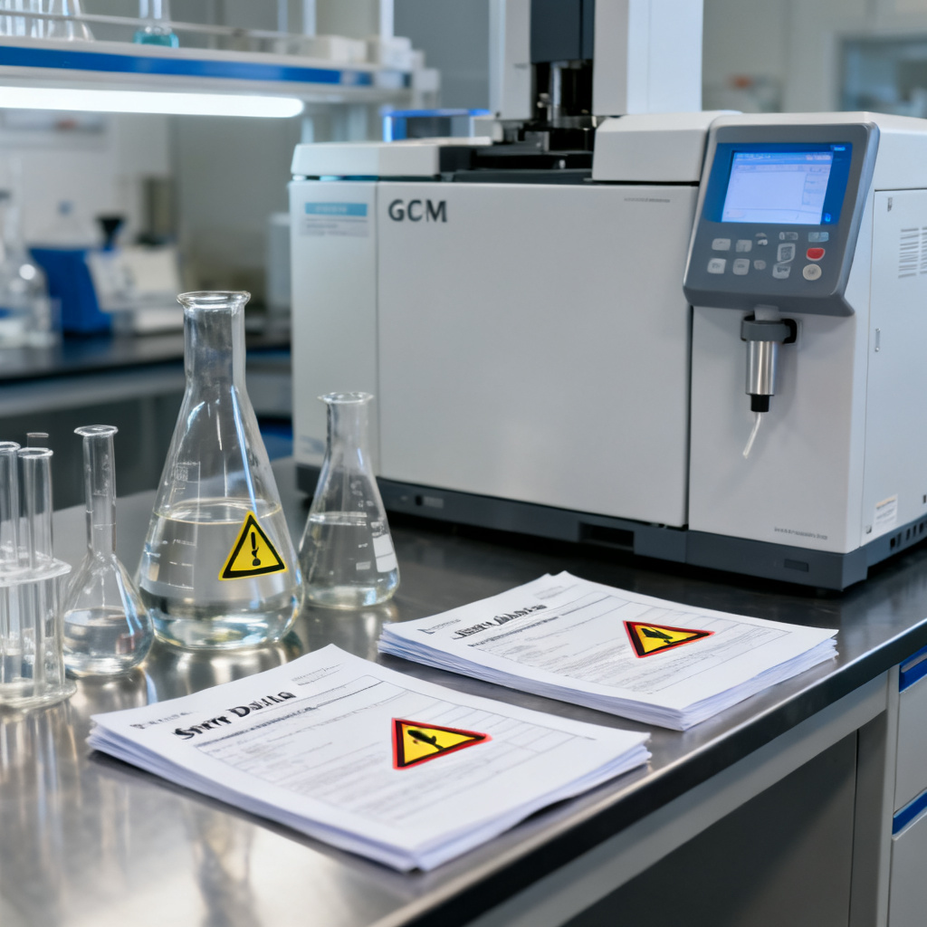
In PCB fabrication, REACH affects raw materials, including resins, hardeners, solvents, and finishing chemicals. For example, some epoxy resins may contain bisphenol A (BPA), which is under scrutiny. Fluxes and cleaning agents must avoid restricted solvents like N‑methylpyrrolidone (NMP). Manufacturers must maintain a Safety Data Sheet (SDS) for every chemical and ensure that SVHCs are not present above 0.1% weight by weight (w/w) in articles. This requires supply chain transparency and regular audits.
Compliance Strategies
To achieve REACH compliance, PCB manufacturers should:
- Implement a chemical management system (e.g., using software like Chemwatch).
- Request REACH declarations from all suppliers.
- Conduct regular testing for SVHCs (e.g., GC‑MS analysis).
- Substitute high‑risk chemicals with greener alternatives (e.g., water‑based fluxes).
- Document all compliance efforts for regulatory inspection.
Halogen‑Free Materials: Reducing Toxic Flame Retardants in Green PCB Manufacturing
Why Halogen‑Free?
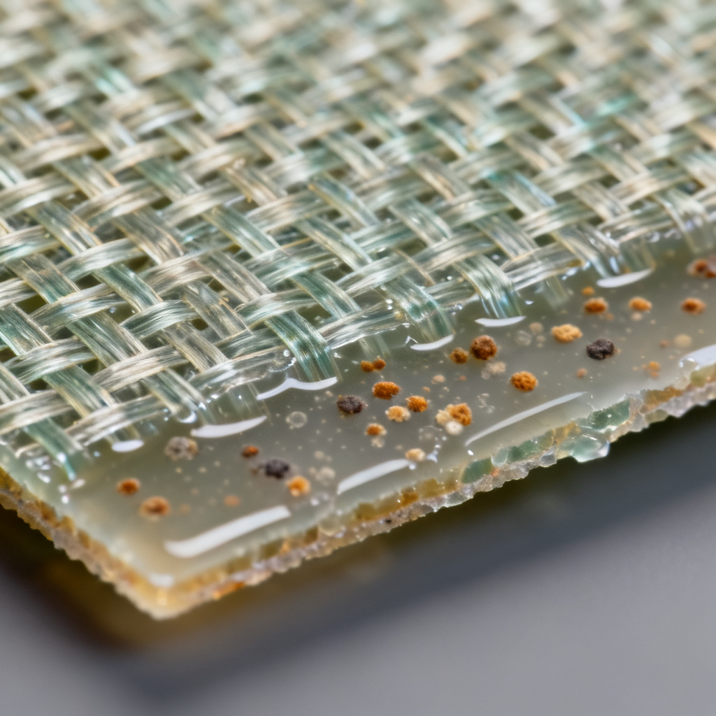
Halogenated flame retardants (e.g., bromine, chlorine) are added to PCB laminates to meet flammability standards (e.g., UL 94 V‑0). However, when burned or disposed of, these materials release toxic gases (e.g., hydrogen bromide, dioxins) that harm human health and the environment. Halogen‑free laminates use phosphorus‑based, nitrogen‑based, or inorganic flame retardants (e.g., aluminum trihydroxide, melamine polyphosphate).
Halogen‑Free Laminate Options
Common halogen‑free PCB materials include:
- FR‑4 variants: Standard FR‑4 can be modified with halogen‑free resin systems (e.g., Isola 370HR, ITEQ IT‑180A).
- Polyimide: High‑temperature polyimide laminates are often inherently halogen‑free.
- PTFE: Used for high‑frequency applications, PTFE laminates are naturally halogen‑free.
- CEM‑3: Composite epoxy materials with halogen‑free options.
Key parameters to consider: glass transition temperature (Tg), thermal conductivity, and dielectric constant (Dk). Halogen‑free laminates may have slightly different mechanical properties, such as higher moisture absorption, requiring careful design.
Verification and Standards
The definition of “halogen‑free” varies: IPC‑4101B specifies a maximum chlorine + bromine content of 1500 ppm (0.15%). IEC 61249‑2‑21 sets a stricter limit of 900 ppm for chlorine and 900 ppm for bromine (total 1800 ppm). Manufacturers should request certification (e.g., IPC‑4101B, UL recognition) and perform ion chromatography (IC) or XRF testing to verify compliance.
E‑waste Management: Closing the Loop in Green PCB Manufacturing
The E‑waste Crisis
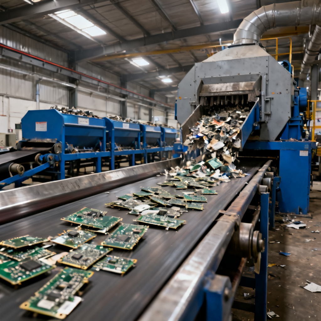
Global e‑waste generation reached 53.6 million metric tonnes in 2019, with only 17.4% officially recycled. PCBs are a major component, containing precious metals (gold, silver, palladium) but also toxic substances (lead, mercury, brominated flame retardants). Improper disposal leads to soil and water contamination, while informal recycling exposes workers to hazards.
PCB Recycling Processes
Effective e‑waste management for PCBs involves:
- Collection and Sorting: Separate PCBs from other e‑waste (e.g., batteries, plastics).
- Dismantling: Remove components (e.g., ICs, connectors) for reuse or recycling.
- Shredding and Separation: Mechanical processes (e.g., hammer mills, eddy current separators) separate metals from non‑metals.
- Pyrometallurgy: High‑temperature smelting to recover gold, copper, and other metals (energy‑intensive but effective).
- Hydrometallurgy: Chemical leaching (e.g., cyanide or thiosulfate) for metal recovery (lower energy, but chemical waste).
- Biomining: Using microorganisms (e.g., Acidithiobacillus ferrooxidans) to extract metals (emerging, eco‑friendly).
Design for Recycling (DfR)
To improve recyclability, PCB manufacturers should:
- Use separable connectors (e.g., JST, Molex) instead of soldered ones.
- Avoid glued or potted components.
- Standardize material types (e.g., single laminate family).
- Provide recycling instructions in product documentation.
- Partner with certified e‑waste recyclers (e.g., R2, e‑Stewards).
Circular Economy Initiatives
Beyond recycling, the circular economy model emphasizes:
- Remanufacturing: Reusing functional PCBs from discarded devices.
- Refurbishment: Repairing and upgrading PCBs for second‑life applications.
- Material Recovery: Closing the loop by using recycled metals (e.g., secondary copper) in new PCB production.
- Product‑as‑a‑Service (PaaS): Shifting from ownership to leasing, incentivizing durability and recyclability.
Integrating Green Practices into PCB Manufacturing
Holistic Sustainability Framework
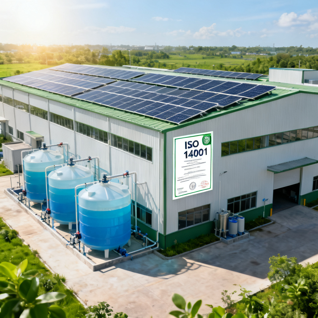
A truly green PCB manufacturer integrates RoHS, REACH, halogen‑free, and e‑waste management into a unified strategy. This includes:
- Green Design: Select materials with low environmental footprint (e.g., halogen‑free laminates, lead‑free finishes).
- Clean Production: Minimize energy and water use, treat wastewater, and use closed‑loop chemical recovery.
- Compliance Assurance: Regular testing and documentation for RoHS, REACH, and halogen‑free standards.
- End‑of‑Life Management: Partner with certified recyclers and offer take‑back programs.
Certifications and Audits
To build trust, manufacturers should obtain certifications such as:
- ISO 14001: Environmental management system.
- ISO 45001: Occupational health and safety.
- UL 94 V‑0: Flammability rating (with halogen‑free option).
- IPC‑4101B: Laminate specification.
- R2 or e‑Stewards: Responsible recycling.
Third‑party audits (e.g., SGS, TÜV) verify compliance and provide transparency.
Case Study: Leading Green PCB Manufacturers
Companies like Unimicron, AT&S, and Ibiden have implemented comprehensive green programs. For example, AT&S uses 100% renewable energy in its Austrian plants and recycles 95% of process water. Unimicron has achieved zero waste‑to‑landfill at several facilities. These examples demonstrate that green manufacturing is both feasible and profitable.
Green PCB Manufacturing: Key Data Table
| Parameter in Green PCB Manufacturing | RoHS | REACH | Halogen‑Free |
|---|---|---|---|
| Primary focus | Substance restriction in finished product | Chemical registration & authorization | Flame retardant composition |
| Key substances | Lead, mercury, cadmium, phthalates | SVHCs (e.g., bisphenol A) | Chlorine, bromine (below 900 ppm each) |
| Compliance testing | XRF, ICP | GC‑MS, supplier declarations | Ion chromatography, XRF |
| Common alternative | SAC305 solder, ENIG finish | Water‑based fluxes, BPA‑free resins | Phosphorus‑based flame retardants |
Industry Terminology in Green PCB Manufacturing
SVHC (Substances of Very High Concern) – chemicals requiring authorization under REACH.
XRF (X‑ray Fluorescence) – a non‑destructive testing method for elemental analysis.
Lead‑free solder – alloys without lead, typically SAC (tin‑silver‑copper).
Halogen‑free laminate – PCB substrate with total halogen < 1500 ppm per IPC‑4101B.
E‑waste – discarded electronic devices; PCBs are a major fraction.
FAQ: Green PCB Manufacturing – RoHS, REACH, Halogen‑Free & E‑waste
What is the difference between RoHS and REACH in green PCB manufacturing?
RoHS restricts specific hazardous substances (e.g., lead, mercury) in finished PCBs, while REACH regulates all chemicals used during manufacturing, including registration of SVHCs. Both are critical for green PCB manufacturing compliance.
Why are halogen‑free materials important for green PCB manufacturing?
Halogen‑free materials reduce toxic gas emissions (dioxins, hydrogen bromide) during combustion or disposal, making PCBs safer for the environment and human health. They are a key component of green PCB manufacturing.
How can I ensure my PCB supplier follows e‑waste management best practices?
Look for certifications like R2 or e‑Stewards, request take‑back programs, and verify that the supplier uses Design for Recycling (DfR) principles. A green PCB manufacturing partner will openly share their e‑waste management policy.