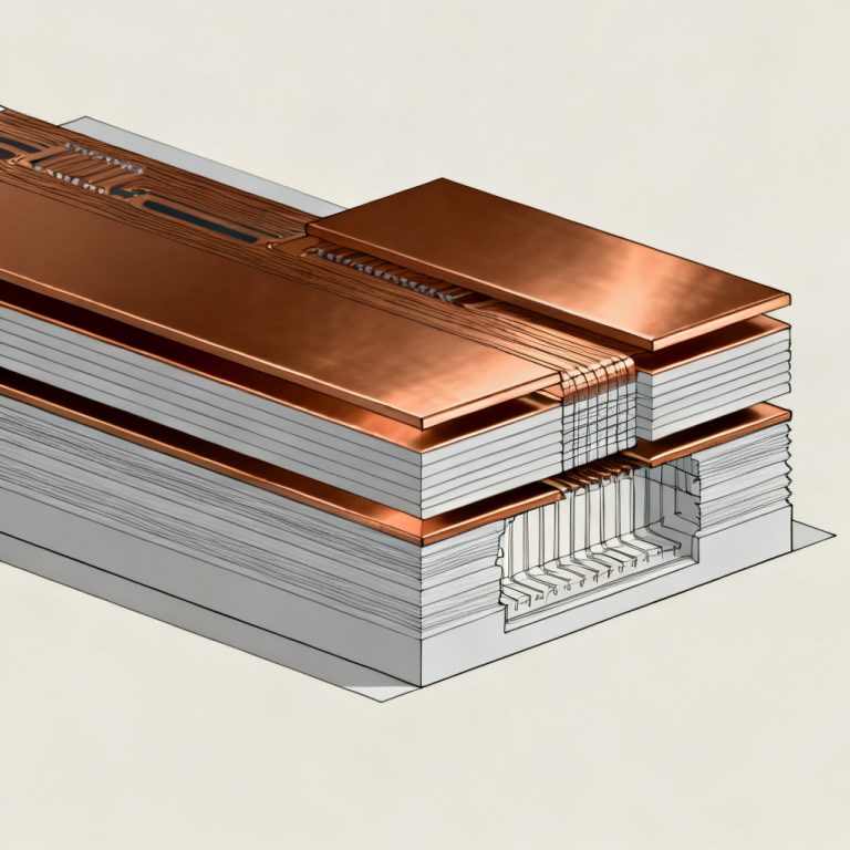
PCB Design & DFX Guidelines: Ultimate DFM/DFA/DFT Guide
This PCB Design DFX DFM DFA DFT Guidelines consolidates the most comprehensive, expert-vetted rules for manufacturable, reliable, and testable printed circuit boards. By following these DFM, DFA, and DFT principles, you will reduce prototype iterations, lower production costs, and ensure first-pass yield for your B2B electronics.
- Core PCB Design Guidelines
- Design for Manufacturing (DFM) Guidelines
- Design for Assembly (DFA) Guidelines
- Design for Testing (DFT) Guidelines
- DFX Integration – Avoiding Common Pitfalls
- DFX Compliance Checklist
- FAQ
1. Core PCB Design Guidelines
These PCB design guidelines focus on fundamental layout rules, stack-up design, and signal integrity for high-speed and general-purpose boards.
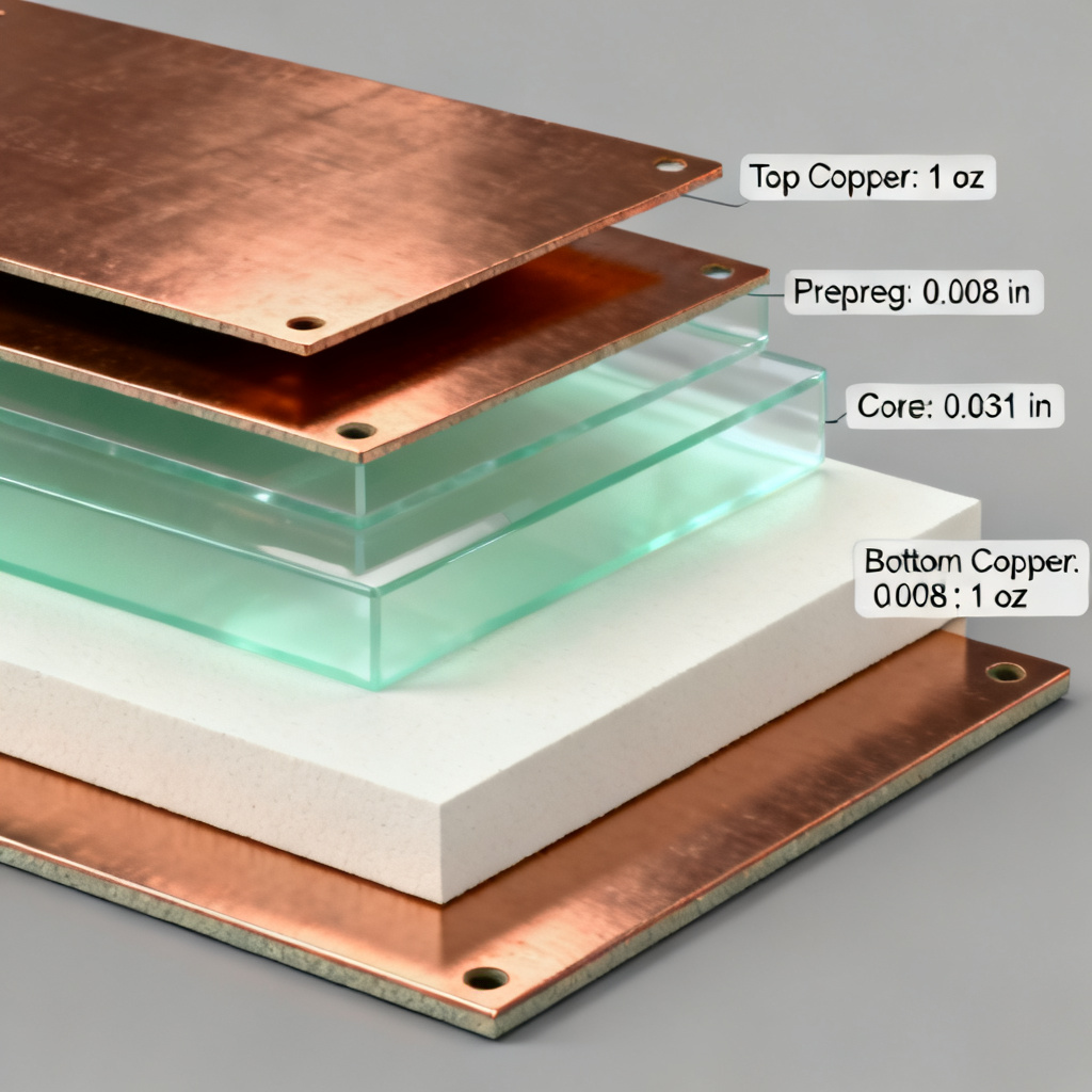
1.1 Layer Stack-Up Design
Symmetry is key: always use a symmetrical stack-up to prevent warpage during lamination and reflow. For example, a 4-layer board should be: Top (Signal) – GND – VCC – Bottom (Signal). For high-speed signals, specify controlled impedance (e.g., 50Ω single-ended, 90Ω differential). Use the manufacturer’s prepreg and core data to calculate trace widths and spacing. Place critical signal layers adjacent to a solid ground plane (usually on a core layer) to minimize return path loops and EMI. Standard 1.6mm boards are common, but for high-layer-count designs (8+ layers), use 1.2mm or 1.6mm with careful dielectric material selection (e.g., FR-4 high Tg, Rogers for RF).
1.2 Trace Routing Rules
For standard signals, use 6–8 mil trace width and 6–8 mil spacing. For high-current paths, calculate width based on IPC-2152 (e.g., 1oz copper, 10°C rise: 100 mil for 3A). For high-voltage, maintain creepage distances (e.g., >40 mil for 250V). Avoid 90-degree corners: use 45° chamfered corners or curved traces to reduce impedance discontinuities and acid traps. For differential pairs, match pair lengths within 5 mils and keep pair-to-pair spacing >5x the pair width to avoid crosstalk. Minimize via count per net to reduce inductance; for high-speed signals, use microvias or back-drilled through-holes to reduce stub effects.
1.3 Component Placement Fundamentals
Place decoupling capacitors (0.1µF and 10µF) as close as possible to IC power pins (within 50 mils). Use multiple vias from pad to ground plane for low inductance. Keep crystal oscillators within 500 mils of the IC and route clock traces on inner layers with ground guard traces. Place connectors at board edges with ESD protection diodes within 100 mils of the connector pins. Use thermal vias under high-power components and avoid placing hot components near temperature-sensitive parts.
1.4 Power Integrity
Use separate power islands for analog and digital sections, connected via a ferrite bead or 0-ohm resistor. Route power from a single source to each load using star topology to minimize shared impedance. Add at least one 100µF electrolytic or tantalum capacitor per power rail at the board entry point.
2. Design for Manufacturing (DFM) Guidelines
These DFM guidelines cover panelization, copper balance, and fabrication constraints used by top PCB fabricators.
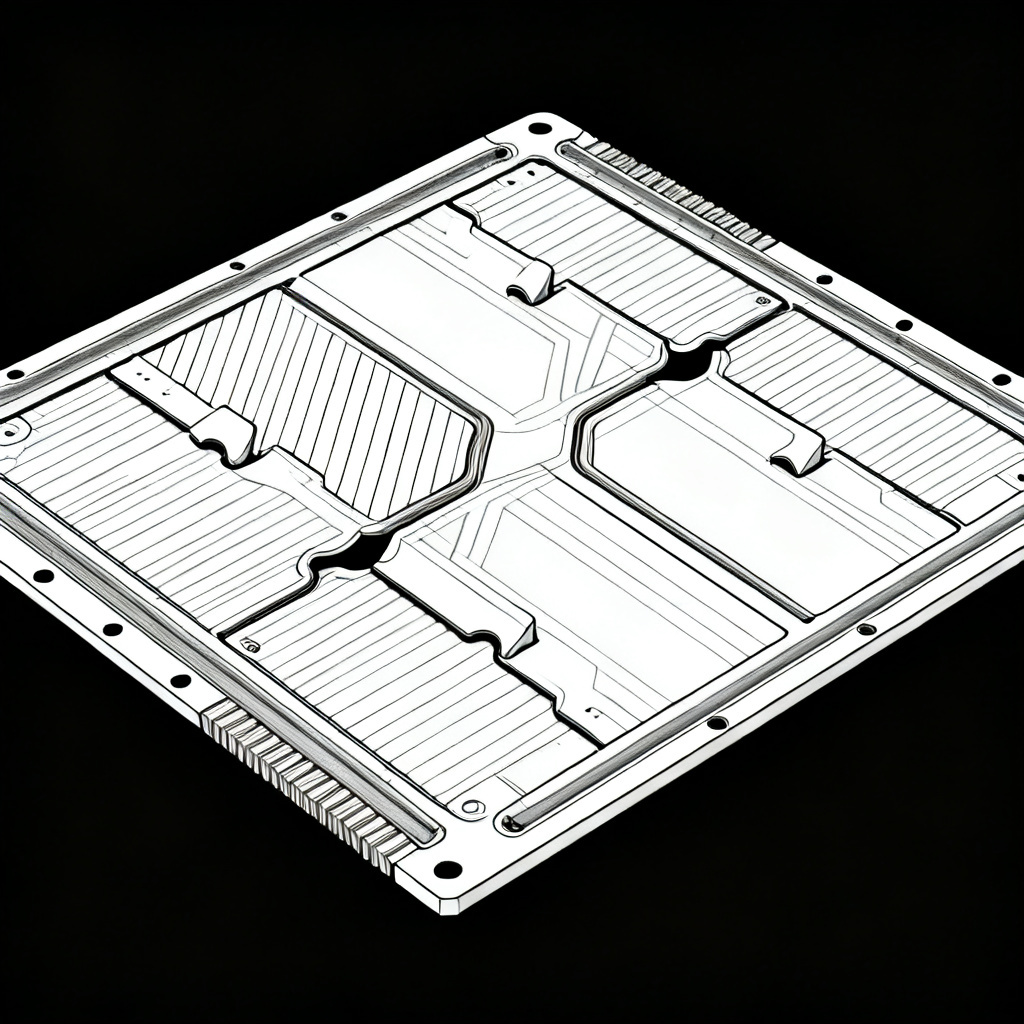
2.1 Panelization Guidelines
Add 5–10mm wide tooling rails on the long sides of the panel for handling. Include 3–5mm tooling holes (non-plated, 3.2mm diameter) at corners. Use V-scoring for rectangular boards with straight edges (depth: 1/3 board thickness). Use tab routing with mouse bites for irregular shapes, leaving at least 1mm clearance between tabs. Add three global fiducials (1mm diameter copper pad with 3mm clearances) at panel corners. For fine-pitch components (0.5mm pitch), add local fiducials within 10mm of the component.
2.2 Copper Balance & Distribution
Maintain >50% copper coverage on outer layers to prevent plating voids. If low copper, add cross-hatched copper pour (e.g., 70% fill, 20 mil grid). Add thieving bars (unconnected copper pads) along panel edges to ensure uniform plating current distribution. Use thermal reliefs for all through-hole pads. For SMD pads, ensure they are connected to a pour or have at least one via to an inner layer.
2.3 Fabrication Tolerances & Constraints
For through-holes, ensure annular ring (pad radius – hole radius) ≥ 6 mil for Class 2, ≥ 8 mil for Class 3. Minimum hole size: mechanical drills 8 mil (0.2mm), laser drills 4 mil (0.1mm). Aspect ratio (board thickness / hole diameter) ≤ 10:1 for through-holes. Use a 2–3 mil solder mask dam between pads for fine-pitch components (e.g., 0.4mm BGA). Minimum solder mask clearance: 2 mil. For RoHS: ENIG (gold) for fine-pitch, HASL-LF for general purpose, OSP for cost-sensitive. Avoid ENIG for high-temperature applications (>200°C) due to black pad risk.
2.4 DFM for High-Volume Production
Use dimensions that fit standard panel sizes (e.g., 18×24 inches). Avoid odd shapes that waste panel space. Minimize layer count: use 2–4 layers for simple designs, 6–8 for moderate complexity, 10+ only for high-density. Each additional layer adds 15–20% cost. Use through-holes unless absolutely necessary; if blind/buried vias are required, limit to 1–2 sequential laminations to reduce cost.
3. Design for Assembly (DFA) Guidelines
These DFA guidelines emphasize SMT assembly, reflow profiling, and manual assembly best practices to avoid tombstoning, solder bridges, and misalignment.

3.1 SMD Pad Design & Stencil
For passive components (0603, 0805), use standard IPC-7351 pad dimensions. For QFNs, use 0.5mm pad width with 0.3mm solder mask opening. Standard stencil thickness: 5 mil (0.127mm) for 0.5mm pitch; 4 mil for 0.4mm pitch (e.g., BGAs); 3 mil for fine-pitch (<0.4mm) with laser-cut stencils. For QFNs, use a 1:1 aperture-to-pad ratio. For BGAs, use 0.9:1 ratio to reduce solder ball bridging. Add 5% area reduction for fine-pitch.
3.2 Component Orientation & Spacing
Place all through-hole components on the top side. For SMD components on the bottom side, orient them so the long axis is parallel to the wave direction to avoid shadowing. For pick-and-place: 0.5mm minimum between SMD components. For rework: 1.5mm clearance around BGA and QFN. For manual assembly: 2mm minimum. Add a silkscreen dot or “1” mark for pin 1 of ICs. For diodes, use a bar on the cathode side. For capacitors, use a “+” sign on the positive side.
3.3 Reflow & Soldering Considerations
Design the board so that all components experience a ramp rate of 1–2°C/sec during preheat, 30–60 seconds above liquidus (217°C for SAC305), and peak temperature of 235–245°C. Avoid placing large thermal mass components near small passives to prevent tombstoning. Use thermal reliefs on large copper areas. For fine-pitch ICs (0.5mm pitch), ensure there is a solder mask dam between pads. For 0.4mm pitch, use a “window” opening (no dam) to allow controlled bridging.
3.4 Through-Hole Assembly
For DIP packages, use 100 mil spacing. For connectors, maintain 2.54mm (100 mil) or 1.27mm (50 mil) pitch. After soldering, leads should protrude 1–1.5mm beyond the board surface. Use lead clinching for high-vibration environments. Ensure the solder fillet covers at least 75% of the pad circumference for through-hole components.
4. Design for Testing (DFT) Guidelines
These DFT guidelines ensure every board can be tested for opens, shorts, and component values during production.
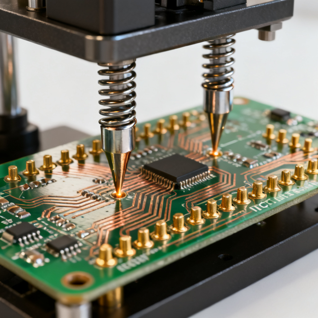
4.1 Test Points (TPs)
Minimum TP size: 35 mil (0.9mm) diameter pad for standard ICT probes; 25 mil (0.6mm) for fine-pitch. Use a 50 mil center-to-center spacing between TPs. Place all TPs on the same side of the board (preferably bottom side) for single-sided probing. Avoid placing TPs under components or within 100 mils of tall components. Add a test point for every net that is not already accessible via a through-hole pin or connector. For critical nets (power, ground, clock), add redundant TPs. Include at least 4–6 ground TPs distributed across the board for probe reference.
4.2 Boundary Scan (JTAG)
For boards with multiple JTAG-compatible ICs (e.g., FPGAs, CPLDs), daisy-chain them in a single JTAG port. Ensure TDI, TDO, TCK, and TMS signals are routed with 50Ω impedance and kept <6 inches. Use JTAG to test interconnects between ICs without physical probing. Add pull-up/pull-down resistors on JTAG lines to ensure known state during testing.
4.3 In-Circuit Test (ICT)
For high-volume production, design the board with 100% TP coverage. Use a vacuum fixture with spring-loaded probes. Ensure the board has at least 4 mounting holes (4mm diameter) for the fixture. Maintain 5mm clearance around TPs for probe contact. Avoid placing TPs near edges (<3mm) to prevent fixture damage. Add a dedicated power TP for each voltage rail. Use a 0-ohm resistor or jumper to isolate power rails during testing.
4.4 Flying Probe Test
For low-volume, use flying probe testers. Ensure all nets are accessible with a 50 mil probe tip. Avoid placing TPs under tall components (>10mm height). Aim for >95% net coverage. Use a netlist-based test to detect opens and shorts. For analog circuits, add test points for voltage measurements.
5. DFX Integration – Avoiding Common Pitfalls
5.1 The “One-Size-Fits-All” Trap
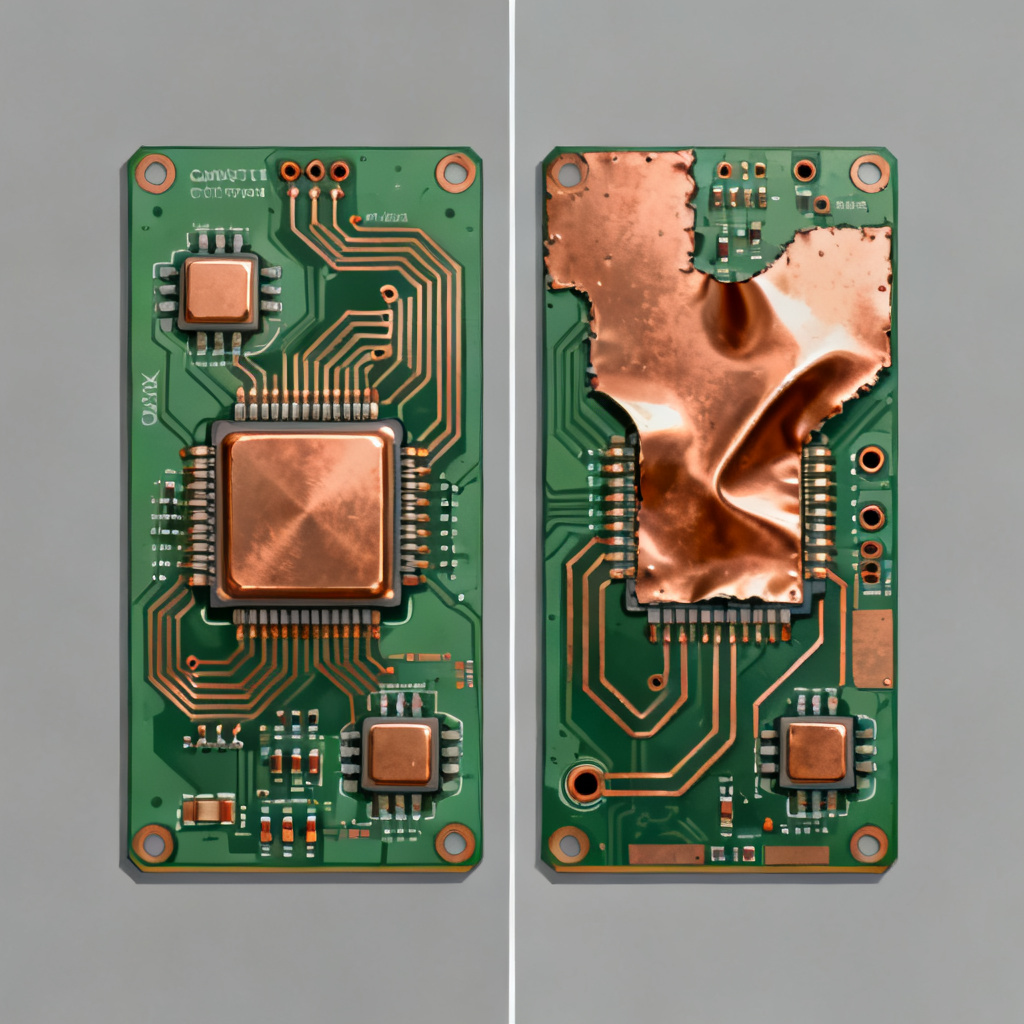
Mistake: Using the same trace width for power and signal. Fix: Use 50–100 mil for power, 6–8 mil for signals. Mistake: Ignoring thermal reliefs on all pads. Fix: Apply thermal reliefs to all through-hole pads and large SMD pads (e.g., QFN exposed pad) to prevent cold solder joints.
5.2 The “Too-Cheap” Design
Mistake: Using 1oz copper for high-current boards. Fix: Use 2oz or 3oz copper for >5A currents. Alternatively, use copper bus bars. Mistake: Skipping solder mask between fine-pitch pads. Fix: Always use solder mask dams for 0.5mm pitch and above.
5.3 The “No-DFT” Design
Mistake: Assuming all nets are testable via connectors. Fix: Add dedicated TPs for every net not exposed on a connector. Mistake: Placing TPs under heat sinks or metal shields. Fix: Relocate TPs to accessible areas.
6. DFX Compliance Checklist
Use this checklist before sending your design to fabrication:
| Category | PCB Design & DFX Guidelines Item | Status |
|---|---|---|
| DFM | Symmetrical stack-up with balanced copper | ☐ |
| DFM | Minimum annular ring ≥ 6 mil | ☐ |
| DFM | Panelized with tooling rails and fiducials | ☐ |
| DFM | No isolated copper islands | ☐ |
| DFM | Solder mask dams for fine-pitch | ☐ |
| DFA | Components spaced ≥ 0.5mm for SMT, ≥ 2mm for manual | ☐ |
| DFA | Polarity marks visible | ☐ |
| DFA | Stencil apertures matched to pad size | ☐ |
| DFA | Thermal reliefs on all through-hole pads | ☐ |
| DFT | Test points on every net (≥35 mil) | ☐ |
| DFT | JTAG chain for complex ICs | ☐ |
| DFT | Ground TPs distributed | ☐ |
| DFT | No TPs under components | ☐ |
| DFA (Assembly) | Component orientation for wave soldering (if applicable) | ☐ |
| DFA (Assembly) | Balanced thermal mass near reflow | ☐ |
| DFA (Assembly) | Lead protrusion 1–1.5mm for through-hole | ☐ |