EMI EMC Compliance Guide for PCB Design – Shielding Filtering
Welcome to the EMI EMC Compliance Guide for PCB Design Shielding Filtering, the ultimate resource for hardware engineers looking to eliminate electrical noise. This comprehensive guide provides expert strategies on shielding and filtering to ensure your board passes compliance certification on the first run.Mastering EMI/EMC compliance is essential for reliable product performance and market approval. This guide consolidates authoritative knowledge from leading industry sources into one definitive resource.
1. Fundamentals of EMI and EMC Compliance for PCB Design
1.1 The Three Elements of EMI
Every EMI/EMC compliance problem involves three components: the source generating interference, the coupling path (conducted or radiated), and the victim (receiver). Effective PCB design must break at least one of these elements to achieve EMI/EMC compliance.
1.2 Common Mode vs. Differential Mode Noise
Understanding noise types is critical for filter selection in EMI/EMC compliance. Differential mode noise appears between two conductors, while common mode noise flows equally on both conductors relative to ground. Common-mode chokes specifically suppress common mode noise without affecting differential signals.
1.3 The Role of Impedance
At high frequencies, PCB traces behave like transmission lines with characteristic impedance. Impedance mismatches cause reflections and radiated emissions, making controlled impedance a key factor in EMI/EMC compliance.
2. Shielding Techniques for PCB Design and EMI/EMC Compliance
2.1 Physical Shield Cans and Enclosures
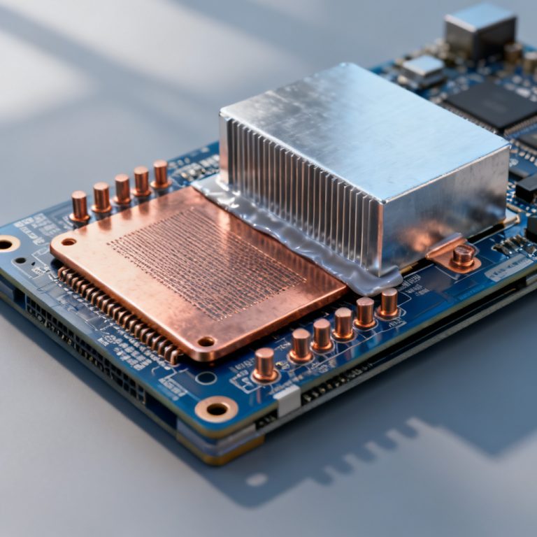
Metallic shield cans placed over noisy or sensitive sections are a direct method for EMI/EMC compliance. Copper, aluminum, or tin-plated steel are common materials. The shield must connect to the PCB ground plane with low impedance, and apertures must be smaller than 1/20th of the wavelength of the highest interfering frequency.
2.2 Ground Planes and Return Paths
A solid, unbroken ground plane is the most effective and cost-efficient shielding technique for EMI/EMC compliance. It provides a low-inductance return path and acts as a shield between layers. Use a dedicated ground plane layer on multi-layer boards, and ensure every high-speed trace has continuous ground beneath it.
2.3 Guard Rings and Via Stitching
Guard rings are copper rings connected to ground that surround sensitive analog circuits, capturing stray currents. Via stitching places ground vias along PCB edges every 1/10th of the wavelength to create a Faraday cage effect, both essential for EMI/EMC compliance.
2.4 Cable and Connector Shielding
Cables act as large antennas. Shielded cables with braided or foil shielding should be terminated to chassis ground at both ends. Metal connectors with 360-degree shield termination provide superior EMI/EMC compliance compared to pigtail wires.
3. Filtering Strategies for EMI/EMC Compliance in PCB Design
3.1 Input/Output (I/O) Filtering
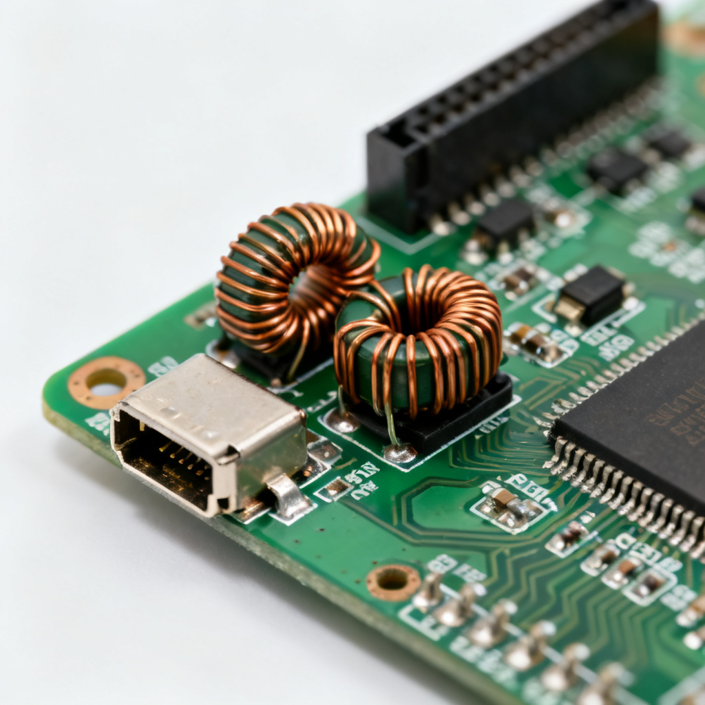
Every I/O line is a potential path for conducted EMI. Ferrite beads placed in series with power lines and signals act as high-impedance elements at high frequencies. Common-mode chokes are essential for differential pairs like USB and Ethernet. Series resistors (10-33Ω) on clock lines dampen ringing and reduce overshoot, improving EMI/EMC compliance.
3.2 Power Supply Decoupling and Bypassing
Power distribution networks carry significant noise. Bulk decoupling capacitors (10-100µF) smooth low-frequency ripple, while small bypass capacitors (0.1µF, 0.01µF) placed within 1-2mm of each IC’s power pin provide local low-impedance current sources. Using X7R or NP0/C0G dielectrics and multiple capacitor values in parallel covers a wide frequency range for optimal EMI/EMC compliance.
3.3 RC and LC Filters
RC low-pass filters are used for slow-speed signals to filter high-frequency noise, with cutoff frequency set above the signal frequency. LC filters are more effective for high-frequency suppression because the inductor presents increasing impedance with frequency. Both are valuable tools in achieving EMI/EMC compliance.
3.4 Filter Placement and Layout
Place filters at the source or victim, keep components close together to minimize loop area, and avoid shared impedance by giving each filter its own dedicated ground connection. These practices are fundamental to EMI/EMC compliance.
4. PCB Layout Best Practices for EMI/EMC Compliance
4.1 Layer Stack-Up Design
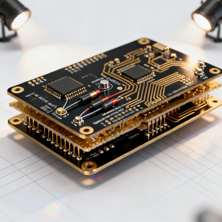
A well-designed stack-up is foundational for EMI/EMC compliance. A 4-layer stack-up (Signal-Ground-Power-Signal) is recommended, with 0.1mm prepreg between signal and ground layers. For 6-layer boards, use Signal-Ground-Signal-Power-Ground-Signal to offer two dedicated ground planes.
4.2 Trace Routing Guidelines
Keep high-speed traces short, maintain consistent width, and separate high-speed from low-speed traces. Use the 3W rule (distance = 3x trace width) between parallel traces to reduce crosstalk. Route differential pairs with equal length and spacing, all critical for EMI/EMC compliance.
4.3 Component Placement
Place noisy components like switching regulators and oscillators near the power entry point and away from connectors. Place sensitive components like analog sensors far from noisy circuits. Keep decoupling capacitors adjacent to ICs with minimal loop area, directly impacting EMI/EMC compliance.
4.4 Grounding Strategy
Use star grounding for low-frequency analog circuits and continuous ground planes for high-frequency digital circuits. For mixed-signal boards, use a single ground plane but physically separate analog and digital sections, connecting them at the ADC/DAC chip. This strategy ensures EMI/EMC compliance across the entire design.
5. Pre-Compliance Testing and Troubleshooting for EMI/EMC Compliance
5.1 Pre-Compliance Testing Methods
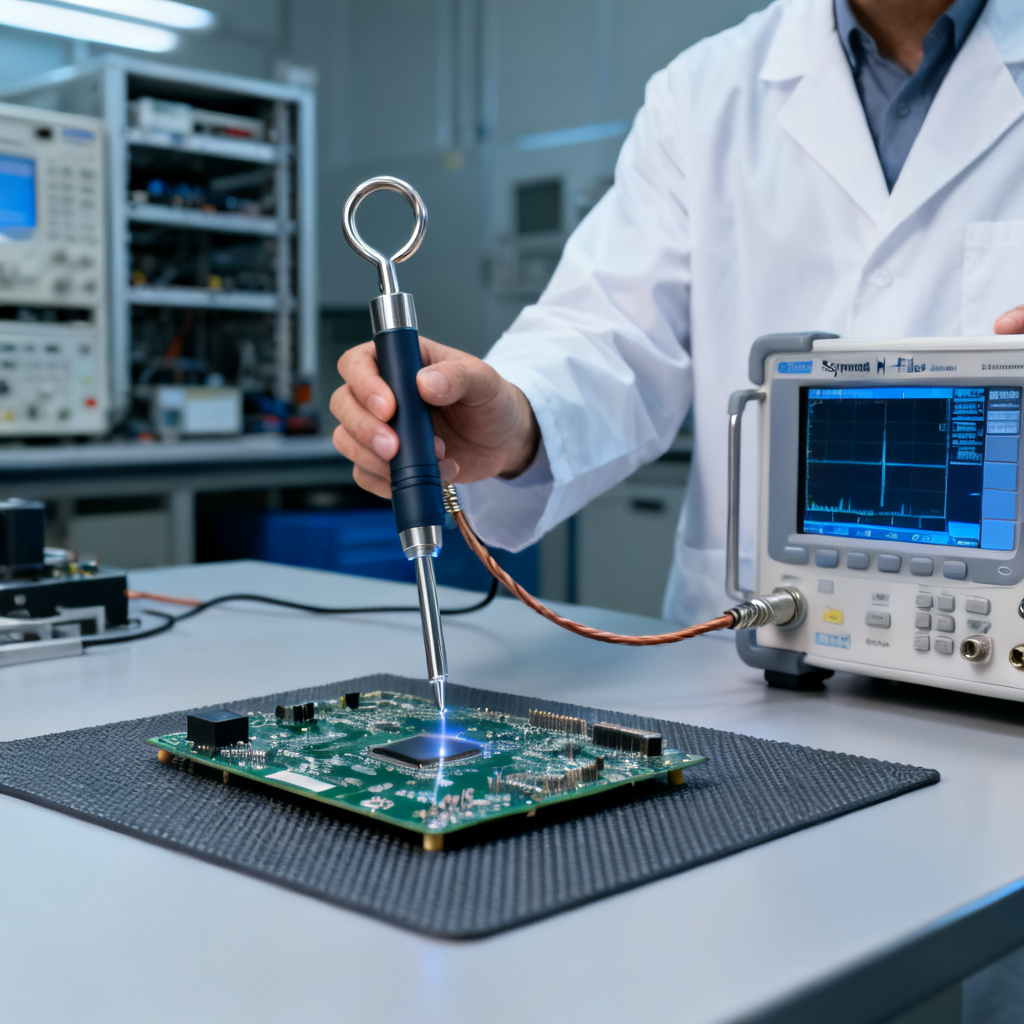
Before lab certification, perform in-house pre-compliance tests using near-field probes connected to a spectrum analyzer for radiated emissions. Use a Line Impedance Stabilization Network (LISN) for conducted emissions. These tests are essential steps toward EMI/EMC compliance.
5.2 Common Problems and Solutions
High radiated emissions from clock traces can be addressed with series resistors and ground planes. Conducted emissions at switching regulator frequencies require improved input filtering and snubber circuits. Noise coupling between digital and analog sections needs increased separation and guard rings. Each solution directly improves EMI/EMC compliance.
5.3 The Role of Layout Iteration
EMC design is iterative. After pre-compliance scans, move components, add shielding, change filter values, or modify routing. Document every change and retest. A methodical approach ensures EMI/EMC compliance and saves time and money.
6. Comparison: Our PCB Manufacturing Advantage for EMI/EMC Compliance
| Parameter | Standard PCB Manufacturer | Our EMI/EMC Compliance Service |
|---|---|---|
| Stack-up support | Basic 2-4 layer | Up to 20-layer with controlled impedance |
| Shielding options | Limited can placement | Custom shield cans, guard rings, via stitching |
| Filtering assistance | Component sourcing only | Full ferrite, choke, and capacitor selection |
| Pre-compliance testing | Not offered | In-house radiated/conducted emissions testing |
| Design review | Basic DFM check | Full EMI/EMC compliance design review |
Frequently Asked Questions About EMI/EMC Compliance for PCB Design
What is the most important step for EMI/EMC compliance in PCB design?
The most important step is establishing a solid ground plane and minimizing loop areas. This foundational technique addresses the majority of EMI/EMC compliance issues by reducing both radiated and conducted emissions.
How do I choose the right shielding material for EMI/EMC compliance?
For high-frequency electric fields, use good conductors like copper or aluminum. For low-frequency magnetic fields, use high-permeability materials like mu-metal. The choice depends on the frequency range of the interference you need to suppress for EMI/EMC compliance.
Can I achieve EMI/EMC compliance on a 2-layer PCB?
Yes, but it is more challenging. Fill unused areas with copper connected to ground with multiple vias, keep traces short, and use careful component placement. For optimal EMI/EMC compliance, a 4-layer board is strongly recommended.
What is the difference between decoupling and bypass capacitors for EMI/EMC compliance?
Decoupling capacitors (bulk, 10-100µF) smooth low-frequency power ripple, while bypass capacitors (small, 0.1µF-1nF) provide local high-frequency current for IC switching transients. Both are essential for EMI/EMC compliance.
How often should I perform pre-compliance testing for EMI/EMC compliance?
Perform pre-compliance testing after each major design revision. Early and frequent testing reduces the risk of failed certification and costly redesigns, ensuring smoother EMI/EMC compliance.